492971
629
Verklein
Vergroot
Pagina terug
1/637
Pagina verder
40055101TH Rev.4 1 / 637
OKIOFFICE44,
OKIFAX 4100/5000 Series
Maintenance Manual
Fourth Edition
2001-08-16
Oki Data Corporation
40055101TH Rev.4 2 /
This manual is intended to be used for installing and maintaining OKIOFFICE44, OKIFAX 4100/5000
series facsimile transceiver.
Maintenance of the OKIOFFICE44, OKIFAX 4100/5000 series is assumed to be conducted at the follow-
ing levels:
Assembly-level maintenance for mechanical portions
Unit-level maintenance for electrical at portions
CAUTION: DANGER OF EXPLOSION IF BATTERY IS INCORRECTLY REPLACED.
REPLACE ONLY WITH THE SAME OR EQUIVALENT TYPE RECOMMENDED BY THE
MANUFACTURER. DISCARD USED BATTERIES ACCORDING TO THE
MANUFACTURER'S INSTRUCTIONS
and
ATTENTION: IL Y A DANGER D'EXPLOSION S'IL Y A REMPLACEMENT INCORRECT DE
LA BATTERIE. REMPLACER UNIQUEMENT AVEC UNE BATTERIE DU MEME TYPE OU
D'UNT TYPE RECOMMANDE PAR LE CONSTRUCTEUR. METTRE AU REBUT LES
BATTERIES USA GEES CONFORMEMENT AUX INSTRUCTIONS DU FABRICANT.
Programming procedures of the following uses's functions are not described in this maintenance manual.
Please refer to user's guide.
One-touch key programming
Two-digit auto dial programming
Group setting
Programming mail box password
Memory operation
ODA/OEL, INT'L MODEL NAME
Note: 5000 series written in this maintenance manual shows OKIFAX 5200, OKIFAX 5300,
OKIFAX 5500, and OKIFAX 5600 model name.
© Copyright 1996 Oki Data Corporation
This manual is subject to alteration without prior notification.
PREFACE
ODA OEL/INT'L
OKIOFFICE44 OKIFAX 4100
OKIFAX 5300 OKIFAX 5200
OKIFAX 5600 OKIFAX 5500
40055101TH Rev.4 3 /
CONTENTS
1.GENERAL INFORMATION...........................................................................................6
1.1 General Performance ...........................................................................................................................6
1.2 General User's Function ......................................................................................................................9
1.3 General Maintenance Functions ..........................................................................................................12
1.4 General Appearance ............................................................................................................................13
1.5 Basic Performance Specifications .......................................................................................................17
1.6 Reports and Lists .................................................................................................................................27
2.INSTALLATION PROCEDURE ................................................................................ 52
A. Setup Information ................................................................................................................................52
2.1 General ................................................................................................................................................52
2.2 Site Selection .......................................................................................................................................54
2.3 Unpacking............................................................................................................................................56
2.3.1 Unpacking for OKIOFFICE44/OKIFAX 4100 ....................................................................56
2.3.2 Unpacking for OKIFAX 5000 Series....................................................................................58
2.4 Check of Contents ...............................................................................................................................61
2.5 Installation of Attachments..................................................................................................................62
2.5.1 Installation of Attachments for OKIOFFICE44/OKIFAX 4100 ..........................................62
2.5.2 Installation of Attachments for OKIFAX 5000 Series..........................................................67
2.6 AC Cord Connection ...........................................................................................................................72
2.7 Telephone and Line Connections ........................................................................................................74
2.8 Packing for Shipment ..........................................................................................................................74
B. Programming and Initial Settings ........................................................................................................75
2.9 Initial Settings......................................................................................................................................75
2.9.1 General Procedure of Key Operation ....................................................................................75
2.9.2 Technical Functions ..............................................................................................................79
2.9.3 Technical Functions Example ...............................................................................................90
2.9.4 User’s Functions ...................................................................................................................97
2.9.5 User's Functions Example .....................................................................................................113
2.9.6 Clock Adjustment .................................................................................................................120
2.9.7 Dual Access Operation (for OKIFAX 5000 series) ..............................................................121
2.9.8 System Data Programming ...................................................................................................122
2.9.9 Dial Parameters Settings .......................................................................................................124
2.9.10 Off-line Tests ........................................................................................................................128
2.9.11 On-line Tests .........................................................................................................................130
C. Installation of Optional Units ..............................................................................................................133
3.BRIEF TECHNICAL DESCRIPTION ........................................................................145
3.1 Fundamentals of the Electro-Photographic Process ............................................................................146
3.2 Actual Electo-photographic Process....................................................................................................148
3.3 Boards and Units .................................................................................................................................149
3.3.1 OKIOFFICE44/OKIFAX 4100 Boards and Units ................................................................149
3.3.2 OKIFAX 5000 Series Boards and Units ...............................................................................149
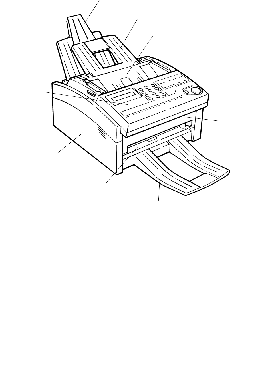
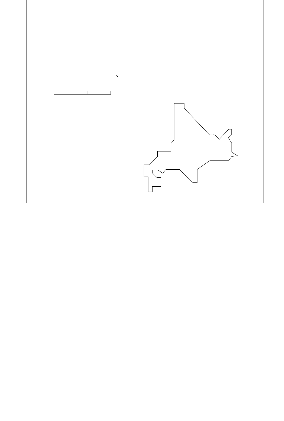
3.4 Overall Dimension and Mechanical Structure of OKIOFFICE44/OKIFAX 4100 .............................152
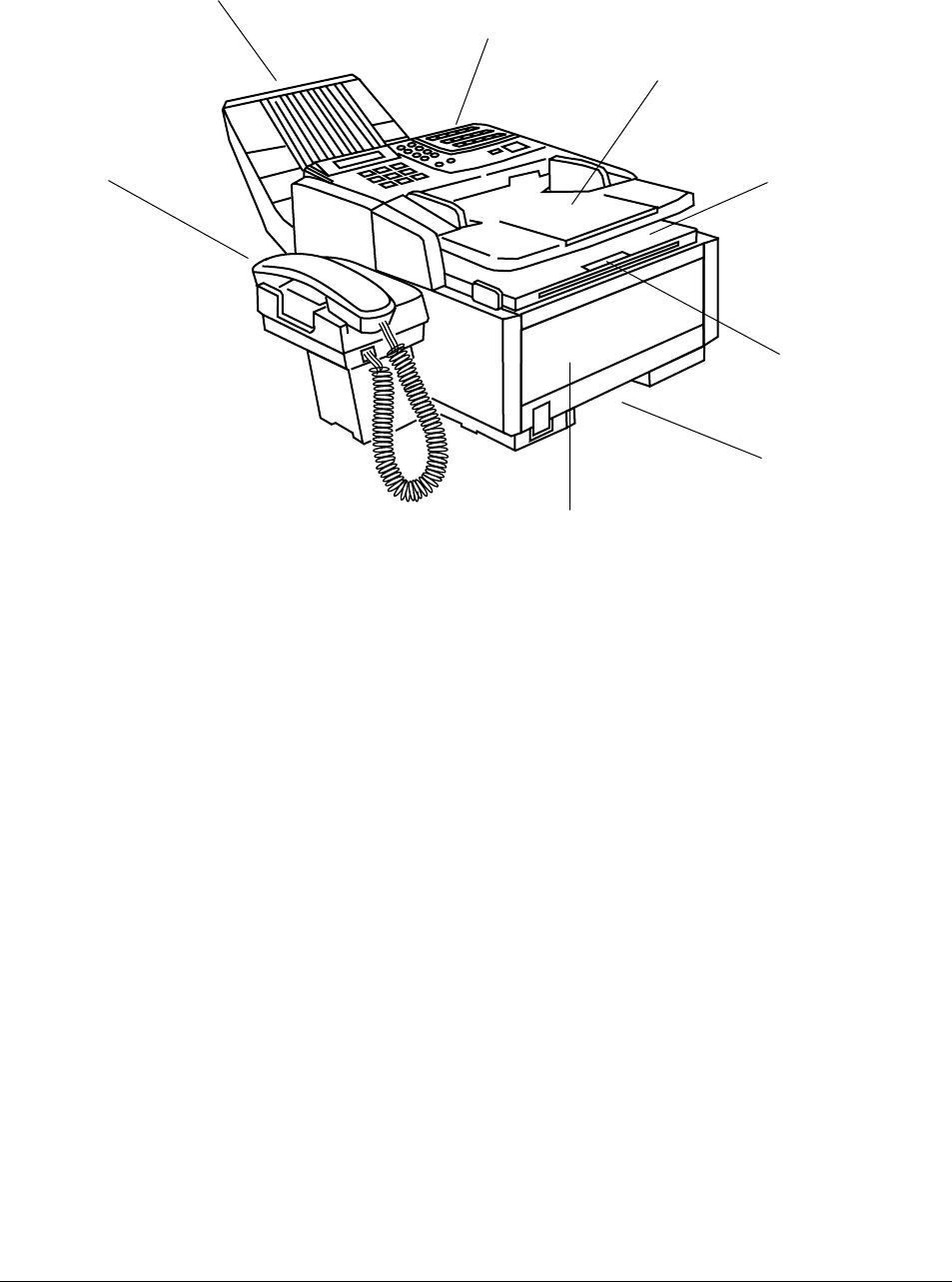
3.5 Overall Dimension and Mechanical Structure of OKIFAX 5000 series .............................................153
4-1.MECHANICAL DISASSEMBLY AND REASSEMBLY
FOR OKIOFFICE44/OKIFAX 4100...................................................................... 154
4.1 General ................................................................................................................................................154
4.1.1 Precautions for Parts Replacement .......................................................................................154
4.1.2 Tools......................................................................................................................................155
4.1.3 How to Disassemble and Reassemble...................................................................................155
4.1.3.1 LED Print Head.......................................................................................................159
4.1.3.2 ID Unit, Rear-Cover, Cover-NCU, Cover-Main and Board-NCU .........................160
4.1.3.3 Unit-048 OPE-Panel ...............................................................................................162
4.1.3.4 Separation Rubber, Roller Assembly Sensor ..........................................................163
4.1.3.5 Roller Assembly-ADF, CIS (contact image sensor), Lever-PC1 and PC2.............164
4.1.3.6 Board-R44, OKIOFFICE 44/OKIFAX 4100 Power Supply Unit ..........................167
4.1.3.7 Option (Board-Memory: MEM, Board-CTR; PC Interface) ..................................168
4.1.3.8 Printer Unit Section.................................................................................................169
4.1.3.9 Transfer Roller ........................................................................................................170
4.1.3.10 High-Voltage Power Supply Unit (TLHV/OLHV) ..............................................171
40055101TH Rev.4 4 /
4.1.3.11 Holder Assembly...................................................................................................172
4.1.3.12 Plate-Side M and Gear-Idle...................................................................................173
4.1.3.13 Registration Roller ................................................................................................174
4.1.3.14 Drive Shaft E (Eject) and Eject Roller ..................................................................175
4.1.3.15 Heat Assembly ......................................................................................................176
4.1.3.16 Pressure Roller B (Back Up Roller)......................................................................177
4.1.3.17 Hopping Shaft Assembly ......................................................................................178
4.1.3.18 Paper Sensor E, Paper Sensor Exit and Toner Sensor Assembly .........................179
4.1.3.19 Printer Unit............................................................................................................180
4-2.MECHANICAL DISASSEMBLY AND REASSEMBLY
FOR OKIFAX 5100 SERIES ................................................................................ 181
4.2 General ................................................................................................................................................181
4.2.1 Precautions for Parts Replacement .......................................................................................181
4.2.2 Tools......................................................................................................................................182
4.2.3 How to Disassemble and Reassemble...................................................................................182
4.2.3.1 LED Print Head.......................................................................................................185
4.2.3.2 ID Unit, Rear Cover, NCU Cover, Main Cover, Separation Plate, NCU Board,
Modem Board .........................................................................................................186
4.2.3.3 Control Panel Assembly, Paper Guide (U) Assembly. ...........................................188
4.2.3.4 Sub-roller, ADF Roller Assembly, Pinch Roller, Contact Image Sensor, Document
Detectors (PC1 and PC2). .......................................................................................190
4.2.3.5 Resist Motor, Drum Motor, Release Guide Assembly, Manual Guide Assembly,
Stacker Cover, Fusing Unit .....................................................................................192
4.2.3.6 Lower Base, Motor Assembly, Back-up Roller, Transfer Roller ...........................194
4.2.3.7 Resist Roller, Hopping Roller, Sensor Plates .........................................................196
4.2.3.8 MCNT Board, Power Supply Unit, Contact Assembly, Transformer, Sub-PSU ...198
5.ADJUSTMENTS ...................................................................................................... 199
5.1 Setting of LED Print Head Drive Time ...............................................................................................199
5.2.1 OKIOFFICE44/OKIFAX 4100 Confirmation Items ............................................................200
5.2.2 OKIOFFICE44/OKIFAX 4100 Measurement ......................................................................201
5.3.1 OKIFAX 5000 Series Confirmation Items ...........................................................................202
5.3.2 OKIFAX 5000 Series Measurement .....................................................................................203
6.CLEANING AND MAINTENANCE ...........................................................................205
6.1 Replacement of Consumable Parts ......................................................................................................205
6.2 Routine Inspection ...............................................................................................................................208
6.2.1 Routine inspection for OKIOFFICE44/OKIFAX 4100 ........................................................208
6.2.2 Routine inspection for OKIFAX 5000 series........................................................................210
6.3 Printer Counter Display/Clear .............................................................................................................212
6.4 Printer Counter Display/Clear .............................................................................................................213
6.5 Self-diagnosis Test ..............................................................................................................................214
6.6 Sensor Calibration Test .......................................................................................................................218
6.7 LED Test .............................................................................................................................................220
6.8 Tone Send Test ....................................................................................................................................221
6.9 High-speed Modem Send Test ............................................................................................................222
6.10 High-speed Modem Receive Test .......................................................................................................224
6.11 MF Send Test ......................................................................................................................................225
6.12 Tone (TEL/FAX) .................................................................................................................................226
6.13 Protocol Dump Data Printing ..............................................................................................................227
6.14 System Reset .......................................................................................................................................231
6.15 Service Code........................................................................................................................................232
7-1.TROUBLESHOOTING AND REPAIR FOR OKIOFFICE44/OKIFAX 4100.......... 235
7.1.1 Overall Troubleshooting Flow Chart...................................................................................................237
7.1.2 No LCD Operation ..............................................................................................................................238
7.1.3 ALARM LED On ................................................................................................................................239
7.1.4 Printing Test Failure ............................................................................................................................240
7.1.5 No Local Copy ....................................................................................................................................241
7.1.6 Auto Dial Failure .................................................................................................................................242
7.1.7 Transmission Problem .........................................................................................................................243
7.1.8 Auto Reception Failure........................................................................................................................245
7.1.9 Reception Problem ..............................................................................................................................246
7.1.10 Sensor Calibration Test .......................................................................................................................248
7.1.11 LED Test .............................................................................................................................................249
40055101TH Rev.4 5 /
7.1.12 Tone Send Test ....................................................................................................................................250
7.1.13 High-speed Modem Test .....................................................................................................................251
7.1.14 MF Send Test ......................................................................................................................................253
7.1.15 Tone (TEL/FAX) Send Test ................................................................................................................254
7.1.16 No Acoustic Line Monitor...................................................................................................................255
7.1.17 Power Supply Unit ..............................................................................................................................256
7.1.18 No Document Feeding.........................................................................................................................265
7.1.19 Multiple Document Feeding................................................................................................................266
7.1.20 Document Skew...................................................................................................................................267
7.1.21 Document Jam .....................................................................................................................................269
7.1.22 Printer Unit ..........................................................................................................................................270
7.1.22.1 Precautions ..........................................................................................................................270
7.1.22.2 Troubleshooting Flow Charts of Printer Unit......................................................................271
7-2.TROUBLESHOOTING AND REPAIR FOR OKIFAX 5000 SERIES .................... 287
7.2.1 Overall Troubleshooting Flow Chart...................................................................................................289
7.2.2 No LCD Operation ..............................................................................................................................290
7.2.3 ALARM LED On ................................................................................................................................291
7.2.4 Printing Test Failure ............................................................................................................................292
7.2.5 No Local Copy ....................................................................................................................................293
7.2.6 Auto Dial Failure .................................................................................................................................294
7.2.7 Transmission Problem .........................................................................................................................295
7.2.8 Auto Reception Failure........................................................................................................................297
7.2.9 Reception Problem ..............................................................................................................................298
7.2.10 Sensor Calibration Test .......................................................................................................................300
7.2.11 LED Test .............................................................................................................................................301
7.2.12 Tone Send Test ....................................................................................................................................302
7.2.13 High-speed Modem Test .....................................................................................................................303
7.2.14 MF Send Test ......................................................................................................................................305
7.2.15 Tone (TEL/FAX) Send Test ................................................................................................................306
7.2.16 No Acoustic Line Monitor...................................................................................................................307
7.2.17 Power Supply Unit ..............................................................................................................................308
7.2.18 No Document Feeding.........................................................................................................................315
7.2.19 Multiple Document Feeding................................................................................................................316
7.2.20 Document Skew...................................................................................................................................317
7.2.21 Document Jam .....................................................................................................................................319
7.2.22 Printer Unit ..........................................................................................................................................320
7.2.22.1 Precautions ............................................................................................................................320
7.2.22.2 Troubleshooting Flow Charts of Printer Unit .......................................................................321
8.DIPSWITCHS SETTING TABLE LIST .....................................................................337
APPENDIX A PC BOARD DESCRIPTIONS AND OPERATION ............................. 361
APPENDIX B1 DESCRIPTIONS OF PRINT OPERATION
(OKIOFFICE44/OKIFAX 4100) ...................................................... 505
APPENDIX B2 DESCRIPTIONS OF PRINT OPERATION (OKIFAX 5000 SERIES)521
APPENDIX C CIRCUIT DIAGRAM AND PARTS LIST .......................................... 541
APPENDIX D1 MECHANICAL EXPANDED VIEW DRAWING AND PARTS LIST
(OKIOFFICE44/OKIFAX 4100).........................................................544
APPENDIX D2 MECHANICAL EXPANDED VIEW DRAWING AND PARTS LIST
(OKIFAX 5200/5300/5500/5600) ......................................................573
APPENDIX E BOARD LAYOUT............................................................................... 600
APPENDIX F SECOND PAPER FEEDER MAINTENANCE MANUAL
(OKIFAX 5000 SERIES) .....................................................................601
APPENDIX G RMCS SYSTEM MANUAL(FOR MODEL 20) ................................... 619
40055101TH Rev.4 6 /
1. GENERAL INFORMATION
1.1 General Performance
(1) Type of appearance
• Desktop type
(2) Applicable lines
• General switched telephone network (GSTN)
• Private branch exchange (PBX)
(3) Compatibility
• ITU-T Group 3 facsimile transceiver
(4) Document width
• Max. 216 mm (NA Letter)
• Min. 148 mm (ISO A5 size)
(5) Effective reading width
• Max. 215 mm
(6) Scanning length
• 128 mm to 356 mm
(Length setting: Infinite is also available.)
(7) Automatic document feeder (ADF)
20 sheets for OKIOFFICE44/OKIFAX 4100 ((NA Letter/A4-size: 20-1b bond. Oki Data recom-
mended paper)
30 sheets for OKIFAX 5000 series (NA Letter/A4-size: 20-1b bond. Oki Data recommended
paper)
• 15 sheets (NA Letter/A4-size: 13 to 28-1b bond)
Note: NA is North America
(8) Recording paper or sheet (Rev. 2)
• 1st tray: NA Letter/NA Legal/A4-size plain paper cut
(OKIOFFICE44/OKIFAX 4100) 100 sheets capacity (20-1b bond*)
• First cassette: NA Letter/NA Legal/A4-size plain paper cut
(OKIFAX 5000 series) 250 sheets capacity (20-1b bond*)
• Second cassette (Option): NA Letter/NA Legal/A4-size plain paper cut
(OKIFAX 5000 series) 500 sheets capacity (20-1b bond*)
• Manual loading feeder: Transparency for overhead projector, applicable.
(OKIOFFICE44, Sheet size: NA Letter/NA Legal/A4-size
OKIFAX 4100/5000 series)
*: Oki Data recommended paper
(9) Printable width
For OKIOFFICE44/OKIFAX 4100
• NA Letter: 203.2 mm (203.2 mm for assured quality)
• NA Legal: 203.2 mm (203.2 mm for assured quality)
• ISO A4: 203.2 mm (197.3 mm for assured quality)
For OKIFAX 5000 series
• NA Letter: 211.3 mm (203.2 mm for assured quality)
• NA Legal: 211.3 mm (203.2 mm for assured quality)
• ISO A4: 206 mm (197.3 mm for assured quality)
(10) Printable length (Rev. 2)
• NA Letter: 273.4 mm (266.7 mm for assured quality)
• NA Legal: 349.6 mm (342.9 mm for assured quality)
• ISO A4: 291 mm (284.3 mm for assured quality)
40055101TH Rev.4 7 /
(11) Copy stacker
• Max. 30 sheets for OKIOFFICE44/OKIFAX 4100 (20-lb bond)
• Max. 100 sheets for OKIFAX 5000 series (20-lb bond)
*: Oki Data recommended paper
(12) Scanning resolution
a) Horizontal:
• 8 pels/mm for OKIOFFICE44/OKIFAX 4100
• 8 pels/mm for OKIFAX 5200/5500 of INT’L version
• 300 dots/inch for OKIFAX 5300/5600 of ODA version
b) Vertical: (Rev. 2)
Transmission mode: 3.85 line/mm (STD), 7.7 line/mm (FINE) or 15.4 line/mm (EX. FINE)
for OKIOFFICE44/OKIFAX 4100 and OKIFAX 5200/5500 of INT’L
version.
3.85 line/mm (STD), 7.7 line/mm (FINE) or 300 dot/inch (EX.FINE) for
OKIFAX 5300/5600 of ODA version.
COPY mode: 7.7 line/mm (FINE) or 15.4 line/mm (EX.FINE) for OKIOFFICE44/
OKIFAX 4100 and OKIFAX 5200/5500 of INT’L version.
7.7 line/ mm(FINE) or 300 dot/inch(EX.FINE) for OKIFAX 5300/5600
of ODA version.
(13) Scanning method
• 1728 bits contact image sensor for OKIOFFICE44/OKIFAX 4100 and OKIFAX 5200/5500 of
INT’L version.
• 2592 bits contact image sensor for OKIFAX 5300/5600 of ODA version.
(14) Recording resolution
a) Horizontal:
300 dots/inch for OKIOFFICE44/OKIFAX 4100/5000 series
b) Vertical: (Rev. 2)
Variable: Automatically adjusted to the paper length.
STD mode (3.85 to 5.06 line/mm) and FINE mode (7.7 to 10.13 line/
mm) for OKIOFFICE44/OKIFAX 4100 and OKIFAX 5200/5500 of
INT’L version.
(300 to 395 dot/inch), STD mode (3.85 to 5.06 line/mm) and FINE mode
(7.7 to 10.13 line/mm) and EX-FINE mode (15.4 to 20.24 line/mm) for
OKIFAX 5300/5600 of ODA version.
Fixed: STD mode: 3.85 line/mm
FINE mode: 7.7 line/mm
EX-FINE mode : 15.4 line/mm
: 300 dot/inch
(15) Recording method
• 211.3 mm (2496 bit) or 216.7 mm (2560 bit)
(16) Minimum scan line time for reception
• When receiving from OKIFAX or ECM: 0 ms
• When receiving from non- OKIFAX and non ECM: 10 ms at 3.85 line/mm
5 ms at 7.7 line/mm
(17) Print speed
• Max. 4 sheets per minute (OKIOFFICE44/OKIFAX 4100)
• Max. 8 sheets per minute (OKIFAX 5000 series)
(18) Pre-heating time
• Approx. 20 sec. for OKIFAX 5000 series (Standby to Print)
• Approx. 30 sec. for OKIOFFICE44/OKIFAX 4100 (Standby to print)
40055101TH Rev.4 8 /
(19) Coding scheme
• Modified Huffman (MH)
• Modified READ (MR)
• Modified Modified READ (MMR)
(20) Modem (Rev. 2)
• ITU-T Rec. V.29: 9600/7200 bps (OKIOFFICE44/OKIFAX 4100/5000 series)
• ITU-T Rec. V.27 ter: 4800/2400 bps (OKIOFFICE44/OKIFAX 4100/5000 series)
• ITU-T Rec. V.21 channel 2: 300 bps (OKIOFFICE44/OKIFAX 4100/5000 series)
• ITU-T Rec. V.17: 14400/12000 bps (OKIOFFICE44/OKIFAX 4100/5000 series)
• ITU-T Rec. V.33: 14400/12000 bps (OKIOFFICE44/OKIFAX 4100/5000 series)
• ITU-T Rec. V.34: 28800 bps (OKIFAX 5500/5600)
Note: 33600 bps (V.34) is available for OKIFAX 5500/5600 when serviceman set to enable.
(21) Transmission speed
• 6 sec. per sheet of ITU-T No. 1 sample document
• 3 sec. per sheet of ITU-T No. 1 sample document
Note: This is Phase C time at 3.85 line/mm and 28800 bps for 3 sec. and 14400 bps for 6 sec. in
MMR code transmission.
(22) Protocol
• ITU-T Rec. T.30
• OKI special protocols: High-speed protocol
(23) Error correction mode (ECM)
(24) Communication mode
• Half duplex
(25) Memory capacity
• Basic model: 256k byte (OKIOFFICE44/OKIFAX 4100/5200/5300)
512k byte (OKIFAX 5500/5600)
• Optional memory: 1M byte memory board can be added. (OKIOFFICE44/OKIFAX 4100,
5200, 5300)
One of 1M byte or 2M byte memory board can be added.
(OKIFAX 5500/5600 series)
(26) Liquid crystal display (LCD)
• Two rows of 20 characters for operation guidance, check and various kinds of information
(27) Power source
• Nominal input voltage 120 VAC for ODA version
• Nominal input voltage 230 VAC for INT’L version
(28) MFP (Multi- Function Peripheral) function (Rev. 2)
• By installing the optional board (CTR board), the MFP function can be realized:
PC Printer Function
PC Scanner Function
PC FaxModem Function
Location Programing Function
Note: For details, see “Product Specification for MFP”
This function is the standard for OKIFAX 5600 and OKIOFFICE44 for ODA.
40055101TH Rev.4 9 /
1.2 General User's Function
(1) Transmit mode
• Automatic transmit mode
• Manual transmit mode
(2) Receive mode
• Automatic receive mode
• Manual receive mode
• TEL/FAX automatic switchover mode
• TAD mode
(3) Dual access (OKIFAX 5000 series)
(4) Voice request
(5) Automatic redial
(6) Last number redial (Manual redial)
(7) Local copy including multiple copies
• Max. 50 copies of document for OKIOFFICE44/OKIFAX 4100 and Max. 99 copies of document
for OKIFAX 5000 series.
(8) Sender identification (Sender ID)
(9) Personal identification (Personal ID)
(10) Polling transmission
(11) Polling reception
(12) Acoustic line monitor
(13) Telephone handset (option)
(14) Automatic alternate selecting call (FAX No. + FAX No. can be registered in one-touch keys).
(15) Delayed transmission (Max. 3 days)
• Delayed broadcast
• Delayed transmission
OKIOFFICE44/OKIFAX 4100; 1 specified time
OKIFAX 5200/5300; 5 specified times
OKIFAX 5500/5600; 20 specified times
(16) Relay broadcast initiate
(17) Confidential message transmission (Hopper 1 station)
(18) Confidential message reception
• OKIFAX 5200/5300: 8 mail boxes
• OKIFAX 5500/5600: 16 mail boxes
(19) PHOTO mode
• OKIOFFICE44/OKIFAX 4100: 16 scale gradations
• OKIFAX 5000 series: 64 scale gradations
(Rev.2)
40055101TH Rev.4 10 /
(20) G3 sequential broadcast (Memory)
• Broadcast mode
OKIOFFICE44/OKIFAX 4100 (56 stations at maximum)
OKIFAX 5200/5300 (84 stations at maximum)
OKIFAX 5500/5600 (134 stations at maximum)
• Delayed broadcast mode
(21) No paper/no toner reception
(22) Memory-only reception (OKIFAX 5000 series)
(Memory reception even if paper does not run out)
(23) Distinguishing Text from picture
(24) Page re-transmission (Only in case of memory TX mode)
(25) Reduction printing (OKIOFFICE44/OKIFAX4100/5300/5600)
Rev.3 (Reduction rate is from 100% to 75%)
(26) Smoothing printing (In case of 3.85 /mm 7.7 /mm)
(27) Programmed key operation (“F” key + “OT” key)
(28) Auto dialing
• One-touch dialing OKIOFFICE44/OKIFAX 4100: 10 locations
OKIFAX 5200/5300: 15 locations
OKIFAX 5500/5600: 30 locations
• Two-digit automatic dialing OKIOFFICE44/OKIFAX 4100: 45 locations
OKIFAX 5200/5300: 64 locations
OKIFAX 5500/5600: 99 locations
• Keypad dialing
• Chain dialing
• Mixed dialing
• Group dialing OKIOFFICE44/OKIFAX 4100: 5 dialing groups
OKIFAX 5200/5300: 10 dialing groups
OKIFAX 5500/5600: 20 dialing groups
(29) Realtime dialing
(In case of optional handset is installed or Hook key)
(30) Automatic pause signal insertion
(31) Manual feeder local copy
(32) Telephone directory (Alpha search) dialing
(33) TEL/FAX automatic switching
(34) Time and date printing
(35) Closed users group (Direct mail rejection)
(36) Transmission contrast and resolution control
(37) Key touch tone
(38) Printer counter display (For drum, toner, total print)
(39) Total page counter (Scan)
(40) Quick scanning 6 sec. minimum A4 size 3.85 /mm for OKIFAX 5200/5300
Quick scanning 3 sec. minimum A4 size 3.85 /mm for OKIFAX 5500/5600
(Rev.2)
(Rev.2)
40055101TH Rev.4 11 /
(41) Date and clock adjustment
(42) PC interface (option)
• Standard: OKIOFFICE44
• Option: OKIFAX 4100/5200/5300/5500/5600
(43) Language selection
• 2 languages (LCD and Reports)
(42) Fax fowarding (for OKIFAX 5500/5600)
(44) Reports
• Activity report
• Protocol report (Service man setting)
• Message confirmation report (Single address or multiple addresses)
• Broad cast entry report (Broadcast)
• Transmission error report
• Confidential reception report
• Configuration report
• Telephone directory
• Power outage report
(Rev.3)
(Rev.2)
40055101TH Rev.4 12 /
1.3 General Maintenance Functions
(1) Self-diagnosis
• CPU ROM/RAM check
• FLASH (/MASK) memory check (Program, Language, Default)
• RAM check
• RAM check (MEMORY board: option)
• PC-IF board (parallel) check
• Print test
(2) Sensor calibration (Adjustment of scanning level)
(3) LED test
(4) Tone send test
(5) Multi-frequency (MF) send test
(6) High-speed modem send test
(7) High-speed modem receive test
(8) Tone (TEL/FAX) test
(9) Remote diagnosis
(10) System reset
(11) Service default report (Machine setting for service engineer)
(Rev.2)
40055101TH Rev.4 13 /
Tray-Paper
Tray-Document
Cover-Top
Case-OPE (T)
Cover-Main
Cover Manual Document
Stacker-Document (O
p
tional)
Cover-Front
1.4 General Appearance
Figure 1.4.1 shows the general appearance of the OKIOFFICE44/OKIFAX 4100.
Figure 1.4.2 shows the general appearance of the OKIFAX 5000 series.
Figure 1.4.3 shows the control panel of the OKIOFFICE44/OKIFAX 4100.
Figure 1.4.4 shows the control panel of the OKIFAX 5200/5300.
Figure 1.4.5 shows the control panel of the OKIFAX 5500/5600.
Figure 1.4.1 General Appearance of OKIOFFICE44/OKIFAX 4100
(FX048 CP4.1 Fig. 01)
40055101TH Rev.4 14 /
Document stacker
Control panel
Document tray
Copy stacker
Sub-paper tray
Recording paper cassette
Manual paper feeder cover
Telephone handset (option)
Figure 1.4.2 General Appearance of OKIFAX 5000 series
40055101TH Rev.4 15 /
Fiture 1.4.3 Control Panel of OKIFAX 4100
UNIQUE
8.5" A4 B5 A5
OKIFAX
AUTO REC SEARCH
AUTO DIAL
HYPHEN
REDIAL
COPY
HOOK
V.REQUEST
PHOTO
EX FINE
FINE STD
LIGHT
NORMAL DARK
ALARM
STOP
START
YES
NO
OKI
*
0
#
ABC DEF
JKL
MNO
GHI
TUV
WXYZ
PQRS
7
8
9
4
5
6
1
2
3
SELECT
FUNCTION
DELAYED
TX
REPORT
PRINT
BROADCAST
FEEDER TX
COUNTER
DISPLAY
CONF.TX
LOCATION
PROG.
RELAY
INIT.-TX
USER
PROG.
POLLNG
MSG. PRINT
FROM MEMORY
10/PAUSE
9/PAUSE8/+7
6
54
321
40055101TH Rev.4 16 /
Fiture 1.4.4 Control Panel of OKIFAX 5000 series
*0#
ABC DEF
JKL MNOGHI
TUV
WXYZPQRS
789
456
123
TONE UNIQUE
8.5" A4 B5 A4
OKIFAX
OKI
0000
AUTO REC
SERCH AUTO DIAL
HYPHEN REDIAL
COPY
HOOK
V.REQUEST
PHOTO RX FINE FINE STD
LIGHT NORMAL DARK
ALARM
STOP START
DELAYED
TX
REPORT
PRINT
BROADCAST
FEEDER TX
COUNTER
DISPLAY
CONF.TX
LOCATION
PROG.
RELAY
INIT.-TX
USER
PROG.
POLLNG
MSG. PRINT
FROM MEMORY
SELECT
FUNCTION
YES
NO
14/SPACE 15/PAUSE
12 34 5
67 89 10
11 12 13/+
40055101TH Rev.4 17 /
1.5 Basic Performance Specifications
Table 1.5.1 shows basic performance specifications.
Note: TF: Technical function setting
FP: Function program setting
OT: One-touch key pressed
F: SELECT FUNCTION key pressed
Table 1.5.1 (1/10) Basic Performance Specifications
No. Item Specifications
Rev.3
Rev.3
1 Applicable line
2 Line interface
1) Impedance
2) Sending power level
3) Receiving power level
3 Type of document to be transmitted
1) Width
2) Length
3) Thickness
4) Shape
5) Opacity
1) General switched telephone network (GSTN)
2) Private branch exchange (PBX) (OT9+2)
600 balanced
0 dBm to 15 dBm range
(Adjustable in 1 dB steps. TF + 22)
6 dBm to 46 dBm
Max. 216 mm (NA Letter)
Min. 148 mm (ISO A5 size)
Note: Effective reading width is NA Letter (215 mm).
Min. 128 mm
Max. 356 mm (14 inches)
Long document detection: 380 mm, or 60 minutes
* TF + 11 (To enable or disable the long document scanning)
Based on common bond paper,
a) 0.08 to 0.13 mm for multiple page feeding
b) 0.06 to 0.15 mm for single page feeding
Rectangular
Documents allowing less than 40% of the scanner source light to
pass through them.
40055101TH Rev.4 18 /
5 Automatic document feeder (ADF)
6 Document skew
7 Document jam detection
8 Document jam removal
Table 1.5.1 (2/10) Basic Performance Specifications
No. Item Specifications
Document width
Communication
Mode/Paper width
Effective reading
width
Copy size
ISO A4 (210 mm)
[INT'L/FTZ]
NA letter (216 mm)
[US/CANADA]
G3/A4
G3/A4
A4
Letter
NA legal (216 mm)
[US/CANADA]
G3/A4
Legal
OKIOFFICE44/OKIFAX 4100
208 mm for TX
200 mm for local copy
OKIFAX 5000 series
208 mm for TX
202.8 mm for local copy
OKIOFFICE44/OKIFAX 4100
215 mm for TX
200 mm for local copy
OKIFAX 5000 series
215.1 mm for TX
211.2 mm for local copy
OKIOFFICE44/OKIFAX 4100
215 mm for TX
200 mm for local copy
OKIFAX 5000 series
215.1 mm for TX
211.2 mm for local copy
Rev.2
Note Local copy: Pritable reading width in local copy mode
Rev.3
4 Effective reading width
Max. 20 documents for OKIOFFICE44/OKIFAX 4100: NA Let-
ter or A4 (20-1b)
Max. 30 documents for OKIFAX 5000 series: NA Letter or A4
(20-1b)
Max. 15 documents: NA Letter or A4 (13-28lb bond paper)
Documents shall be placed facedown on ADF stacker.
The first sheet will be fed first in the feeder and will exit facedown
in the document stacker.
Max. 2.6 mm skew over a document of A4 length.
For a document longer than A4 length, occurrence of skew
exceeding 2.6 mm over any A4 length is 0.5% or less.
1) Transmission will stop and line disconnection will occur when
the end of a document is not detected within 356 mm after
scanning begins (except for the long document scanning. TF
+ 11)
2) A jam will also be declared if the document does not reach the
scanning position within 5.5 seconds (OKIFAX 5000 series)/
10 seconds (OKIOFFICE44/OKIFAX 4100) after the start of
a document feed.
Note: When a jam is detected during message transmission from
the feeder, the machine will stop scanning and disconnect
the line, but its receiving capability will remain valid.
Manual release
40055101TH Rev.4 19 /
Table 1.5.1 (3/10) Basic Performance Specifications
No. Item Specifications
9 Recording paper or sheet
10 Recording paper cassette
1) First tray
(For OKIOFFICE44/
OKIFAX 4100)
2) First cassette
(For OKIFAX 5000 series)
3) Second cassette (Option)
(For OKIFAX 5000 series)
For the first or second recording paper cassette:
1) Type: Plain paper cut (Bond paper)
2) Size: ISO A4 (210 mm x 297 mm)
NA Letter (215.9 mm x 279.4 mm)/(8.5 inch x 11
inch)
NA Legal (215.9 mm x 355.6 mm)/(8.5 inch x 14
inch)
3) Weight: 16 lbs to 24 lbs/base weight
Base weight is defined as the weight of 500 sheets
of 431.8 mm (17 inch) by 558.8 mm (22 inch).
4) Thickness:0.08 mm to 0.12 mm
5) Condition: New paper
For the manual loading feeder on the first cassette:
(OKIOFFICE44/OKIFAX 4100/5000 series)
1) Type: Plain paper, transparency for overhead projector,
colored paper, printed paper
2) Size: A4/NA Letter/NA Legal
3) Weight, thickness and condition: Same as above
Note: One single sheet only should be loaded on the manual
loading feeder for any one occasion.
For best results use Oki Data recommended papers
1) Xerox 4200 (20 - lb/base weight paper)
2) L-type paper for photo-printers
100 sheets/tray (Oki Data recommended paper)
250 sheets/cassette (Oki Data recommended paper)
500 sheets/cassette (Oki Data recommended paper)
40055101TH Rev.4 20 /
Table 1.5.1 (4/10) Basic Performance Specifications
No. Item Specifications
2) Guaranteed printing area
Printing area
EL
PL
B
T
L
R
PW
EW
Recording
paper
feed
direction
(F050-C1-001)
For OKIOFFICE44/OKIFAX 4100:
1) Printable area
PL 11 279.4 11.7 297 14 355.6
inch mm inch mm inch mm
NA LETTER SIZE ISO A4 SIZE 14 inch LEGAL SIZE
PW 8.5 216 8.27 210 8.5 216
EL 10.76 273.4 11.46 291 13.76 349.6
EW 8.0 203.2 8.0 203.2 8.0 203.2
T 0.12 3 0.12 3 0.12 3
B 0.12 3 0.12 3 0.12 3
L 0.25 6.35 0.13 3.4 0.25 6.35
R 0.25 6.35 0.13 3.4 0.25 6.35
13 inch LEGAL SIZE
13
inch
mm
8.5
12.76
8.0
0.12
0.12
0.25
0.25
330.2
216
324.2
203.2
3
3
6.35
6.35
PL 11 279.4 11.7 297 14 355.6
inch mm inch mm inch mm
NA LETTER SIZE ISO A4 SIZE 14 inch LEGAL SIZE
PW 8.5 216 8.27 210 8.5 216
EL 10.5 266.7 11.2 284.3 13.5 342.9
EW 8.0 203.2 7.77 197.3 8.0 203.2
T 0.25 6.35 0.25 6.35 0.25 6.35
B 0.25 6.35 0.25 6.35 0.25 6.35
L 0.25 6.35 0.25 6.35 0.25 6.35
R 0.25 6.35 0.25 6.35 0.25 6.35
13 inch LEGAL SIZE
13
inch
mm
8.5
12.5
8.0
0.25
0.25
0.25
0.25
330.2
216
317.5
203.2
6.35
6.35
6.35
6.35
Rev.2
11 Effective recording area
Note: These tables do not
include vertical and horizon-
tal addressing deviations (+
or 2 mm) of recording paper.
40055101TH Rev.4 21 /
Table 1.5.1 (5/10) Basic Performance Specifications
No. Item Specifications
12 Copy stacking
13 Scanning resolution
For OKIOFFICE44/OKIFAX 4100:
The fax can discharge printed copies and stack them faceup.
Maximum sheets on the copy stacker: 30*
For OKIFAX 5000 series:
The fax can discharge printed copies and stack them facedown.
Maximum sheets on the copy stacker: 100*
Note*:Oki Data recommended paper
Horizontal:
8 pel/mm for OKIOFFICE44/OKIFAX 4100 and OKIFAX
5200/5500 of INTL version.
300 dot/inch for OKIFAX 5300/5600 of ODA version.
Vertical:
Transmission mode:
3.85 line/mm (STD), 7.7 line/mm (FINE) or 15.4 line/mm
(EX. FINE) for OKIFAX 4100 and OKIFAX 5200/5500 of
INTL version.
3.85 line/mm (STD), 7.7 line/mm (FINE) or 300 dot/inch,(EX.
FINE) for OKIFAX 5300/5600 of ODA version.
COPY mode:
7.7 line/mm (FINE) or 15.4 line/mm (EX.FINE) for
OKIOFFICE44/OKIFAX 4100 and OKIFAX 5200/5500 of
INTL version.
7.7 line/ mm(FINE) or 300 dot/inch(EX. FINE) for
OKIFAX5300/5600 of ODA version.
For OKIFAX 5000 series:
1) Printable area
PL 11 279.4 11.7 297 14 355.6
inch mm inch mm inch mm
NA LETTER SIZE ISO A4 SIZE 14 inch LEGAL SIZE
PW 8.5 216 8.27 210 8.5 216
EL 10.5 266.7 11.2 284.3 13.5 342.9
EW 8.0 203.2 7.77 197.3 8.0 203.2
T 0.25 6.35 0.25 6.35 0.25 6.35
B 0.25 6.35 0.25 6.35 0.25 6.35
L 0.25 6.35 0.25 6.35 0.25 6.35
R 0.25 6.35 0.25 6.35 0.25 6.35
13 inch LEGAL SIZE
13
inch
mm
8.5
12.5
8
0.25
0.25
0.25
0.25
330.2
216
317.5
203.2
6.35
6.35
6.35
6.35
2) Guaranteed printing area
PL 11 279.4 11.7 297 14 355.6
inch mm inch mm inch mm
NA LETTER SIZE ISO A4 SIZE 14 inch LEGAL SIZE
PW 8.5 216 8.27 210 8.5 216
EL 10.76 273.4 11.46 291 13.76 349.6
EW 8.32 211.3 8.11 206 8.32 211.3
T 0.12 3 0.12 3 0.12 3
B 0.12 3 0.12 3 0.12 3
L 0.09 2.3 0.08 2 0.09 2.3
R 0.09 2.3 0.08 2 0.09 2.3
13 inch LEGAL SIZE
13
inch
mm
8.5
12.76
8.32
0.12
0.12
0.09
0.09
330.2
216
324.2
211.3
3
3
2.3
2.3
Rev.2
40055101TH Rev.4 22 /
Table 1.5.1 (6/10) Basic Performance Specifications
No. Item Specifications
Rev.2
Rev.2
Rev.3
14 Image scanning method
15 Contrast control
16 Recording resolution
17 Recording system
18 Skew of recording paper
19 Copy darkness
20 Copy uniformity
21 Recording paper running out
22 Minimum scan line time for receiving
23 Coding scheme
NA Letter size (1728-bit) contact image sensor for OKIOFFICE44,
OKIFAX4100/5200/5500
NA Letteer size (2592-bit) contact image sensor for OKIFAX 5300/
5600
1) Automatic background sensing
A continuous document background of 0.3 OD (optical density)
or less will be transmitted as white.
2) The LIGHT and DARK contrasts will automatically be adjusted
to improve image quality.
Horizontal:
300 dot/inch
Vertical:
3.85 line/mm (STD), 7.7 line/mm (FINE) for OKIOFFICE44/
OKIFAX 4100 and OKIFAX 5200/5500 of INTL version.
3.85 line/mm (STD), 7.7 line/mm (FINE), 300 dot/inch (FX-
FINE) for OKIFAX 5300/5600 of ODA version.
Electro-photographic printing
1) 211.3mm (2496 bit) or 216.7mm (2560 bit) LED print head
Maximum allowable skew is + or - 1 mm over an advance of 100 mm.
1) Black image: Greater than 1.0 OD (Optical density)
2) White background: Not greater than 0.2 OD
(Optical density)
Printed copies will exhibit a uniform density of the printed and
background area:
1) From edge to edge: 25% unit
2) From copy to the next copy: 30% unit
The fax can detect the no-paper condition by a photosensor.
When the paper has run out in the local copy operation, the scanning
will stop with NO PAPER ... REPLACE PAPER on the LCD for
OKIFAX 5000 series and PAPER OUT/JAM on the LCD for
OKIOFFICE44/OKIFAX4100 and an ALARM LED turns on with-
out an alarm tone.
When the paper has run out while a message is being received and
the no-paper reception is activated, the LCD display will show
MSG. IN MEMORY, and the ALARM LED turns on.
0 ms, when receiving from an Oki Data facsimile.
5 ms at 7.7 line/mm and 10 ms at 3.85 line/mm when receiving from
a non-Oki Data facsimile.
1) One-dimensional coding scheme:
Modified Huffman (MH)
2) Two-dimensional coding scheme:
Modified READ (MR)
Modified modified READ (MMR)
40055101TH Rev.4 23 /
a) ITU-T Rec. V.29 (9600/7200 bps)
b) ITU-T Rec. V.27 ter (4800/2400 bps)
c) ITU-T Rec. V.17 (14400/12000/9600/7200 bps)
d) ITU-T Rec. V.33 (14400/12000 bps)
e) ITU-T Rec. V.34 (28800 bps); for OKIFAX 5500/5600
Note: 33600 bps (V.34) is available for OKIFAX 5500/5600
when serviceman set to enable.
ITU-T Rec. V.21 channel 2 (300 bps)
Automatic fallback will occur according to the following sequence
by FTT, RTN or PPR.
When the last trial fails, the transmitting station sends out a DCN
signal to the remote station for disconnection.
Note 1: Continuous PPRs for the same partial page within each
fallback rank.
1) ITU-T Rec. T.30
2) Oki Data special protocol
High-speed protocol
The T.30 protocol signal from the transmitting station is sent at
message transmission speed instead of 300 bps.
Note: In high-speed protocol, 28.8 K-bps are not supported.
Note 2: V.34 modern performs the fall-back depending upon the
line condition automatically.
Table 1.5.1 (7/10) Basic Performance Specifications
No. Item Specifications
Rev.2
Rev.2
Fallback
rank
1st
2nd
3rd
4th
5th
6th
Transmission
speed
14400 bps
12000 bps
9600 bps
7200 bps
4800 bps
2400 bps
Activated by
FTT (Times)
1
1
1
1
2
2
Activated by
RTN (Times)
1
1
1
1
1
1
Activated by
PPR (Times)
4 (Note 1)
4 (Note 1)
4 (Note 1)
4 (Note 1)
4 (Note 1)
4 (Note 1)
Protocol
ITU-T V.17 (V.33)
ITU-T V.17 (V.33)
ITU-T V.17 (V.29)
ITU-T V.17 (V.29)
ITU-T V.27 ter.
ITU-T V.27 ter.
1st
2nd
3rd
4th
5th
6th
7th
8th
9th
10th
11th
12th
1 (Note 1)
1 (Note 1)
1 (Note 1)
1 (Note 1)
1 (Note 1)
1 (Note 1)
1 (Note 1)
1 (Note 1)
1 (Note 1)
1 (Note 1)
1 (Note 1)
1 (Note 1)
ITU-T V.34
ITU-T V.34
ITU-T V.34
ITU-T V.34
ITU-T V.34
ITU-T V.34
ITU-T V.34
ITU-T V.34
ITU-T V.34
ITU-T V.34
ITU-T V.34
ITU-T V.34
28800 bps
26400 bps
24000 bps
21600 bps
19200 bps
16800 bps
14400 bps
12000 bps
9600 bps
7200 bps
4800 bps
2400 bps
Fallback rank
Transmission speed
Activated byPPR (Times)
Protocol
24 MODEM
1) High-speed MODEM
2) Low-speed MODEM
25 Fallback
26 Protocol
40055101TH Rev.4 24 /
28 Error correction
29 Communication mode
30 Ringing signal detection sensitivity
1) Voltage range
2) Frequency range
3) Ring response time
31 Image memory
32 Telephone handset
(option)
Rev.2
Table 1.5.1 (8/10) Basic Performance Specifications
No. Item Specifications
OKIOFFICE44/OKIFAX 4100
OKIFAX 5200/5300
OKIFAX 5500/5600
Basic model
256K-byte
256K-byte
512K-byte
Optional memory
1M-byte
1M-byte
1M-byte/2M-byte
Memory
condition
OKIFAX 4100
OKIOFFICE44
[pages]
OKIFAX
5200/5300
[pages]
OKIFAX
5500/5600
A4 Setting
[pages]
Standard
(without option)
With
option
board
1M-byte
2M-byte
20
100
20
100
120
200
*
1
CTR board is not mounted.
*
2
CTR board is mounted.
5500: 30*
1
5500: 26*
2
5600: 38
Rev.2
27 Transmission time
3 sec.(approx 3.5 sec) /ITU-T No. 1 sample document
(OKIFAX 5500/5600)
6 sec.(approx 6.9 sec) /ITU-T No. 1 sample document
(OKIOFFICE44, OKIFAX 4100/5000 series)
Note: This is Phase C time at 3.85 line/mm and 28800 bps for 3
sec. and 14400 bps for 6 sec. in MMR code transmission.
ITU-T Error correction mode (ECM)
Oki Data ITU-T ECM
Half-duplex
25 to 150 V r.m.s.
Inoperative below 10 V
20 to 68 Hz
One-ringing signal or 5 to 30 seconds.
(Selectable in 5 sec. steps. F + OT9 + + 11)
Note: ITU-T No.1 sample document is used to count the num-
ber of sheets.
Back-up time on electrical interruption:
Min. one hour (OKIFAX 5000 series with option memory)
Note: OKIOFFICE44/OKIFAX 4100 and OKIFAX 5000 se-
ries without option memory does not back up the message
received in memory for the power failure.
General telephone function is available while the power is on.
Note: In the fax special versions, general telephone is available
even when the power is off.
40055101TH Rev.4 25 /
34 Overheat protection
35 PC interface applications (Option)
Note: This function is the standard
for OKI OFFICE44.
36 Power supply unit and power consump-
tion of the machine
Rev.3
Table 1.5.1 (9/10) Basic Performance Specifications
No. Item Specifications
Rev.3
OKIFAX 4100OKIOFFICE44
OKIFAX
5200/5500
OKIFAX
5300/5600
Power consumption of the machine
(Typical power)
Transmit
Receive
Local copy
19W
115W
150W
10W
21W
112W
150W
10W
0.5W
Standby
(Power Save OFF)
Standby
(Power Save ON)
60W
160W
210W
16.6W
0.5W
60W
160W
210W
16.6W
** OKIOFFICE44 has standard PC interface,
therfore has no power save mode.
OKIFAX5300/5600 has no power
save mode.
The heater of the fuser unit is controlled within the predetermined
temperature range by the thermistor. If the temperature of the heater
exceeds the range, the LCD displays PRINTER ALARM 4.
Furthermore, the built-in thermostat in the fuser unit prevents the
heater from being overheated even in the event of the failures in the
above temperature control circuit.
The following four modes are supported:
1) PC local printer function
2) PC scanner function
3) PC FaxModem function
4) Location Programing function
Note: This function will be supplied as the OKIFAX 4100/5200/
5300/5500/5600 option in case Oki Data can get the
approval in respective countries without modifying the
optional unit.
For, details, see product specification for MFP.
37 Ambient condition
1) Operating condition
2) Storage condition
See Figure 1.5.1
See Figure 1.5.1
40055101TH Rev.4 26 /
Table 1.5.1 (10/10) Basic Performance Specifications
No. Item Specifications
0
10
20
30
40
50
60
70
80
90
10 20 30 40
0°C10%
18°C
27°C
28°C
15°C20%
43°C10%
43°C
43°C29%
32°C20%
32°C54%
10°C30%
0°C64%
73%
10°C73%
18°C80%
28°C85%
27°C80%
15°C
TEMPERATURE [
°C]
Relative humidity [%RH]
Area enclosed by lines with : Range where printing is guaranteed.
Area enclosed by lines with : Range for storage without power supply.
85%
(Note) The curve connecting 28°C, 85% and 0°C, 64%
is the condensation curve.
Temperature and Humidity Conditions
Figure 1.5.1 Ambient Conditions
Rev.2
For OKIOFFICE44/OKIFAX 4100:
1) Width: Approx. 312 mm
2) Depth: Approx. 383 mm
3) Height: Approx. 190 mm
OKIFAX 5000 series:
1) Width: Approx. 330 mm
2) Depth: Approx. 420 mm
3) Height: Approx. 245 mm
Approx. 8 kg for OKIOFFICE44/OKIFAX 4100
Approx. 13 kg for OKIFAX 5000 series
Excluding optional units, recording paper and packing materials.
1) AC power cord x 1
2) I/D unit x 1 (Already installed)
3) Toner cartridge x 1
4) Telephone handset x 1 (option)
5) Curled cord and Telephone cord for (4) x 1 (option)
6) Document stacker x 1
7) Line cord x 1
8) One touch sheet x 1 (Already installed)
9) Users guide x 1
38 Dimension
(Main body)
39 Weight
(Main body)
40 Attachment
(to the main body)
40055101TH Rev.4 27 /
The transmitter sends a call-back message to the receiver only
when the receiver does not respond to voice request of the transmit-
ter.
The fax can transmit a programmed alphanumeric message, such as
company’s name, consisting of up to 32 characters.
* (Outside only)
Received TSI can be printed at the top of the received page.
* TF + 05 (To enable or disable this function)
The fax can automatically print out a power-outage report when the
power off condition occurs.
The fax can print out an activity report manually, and provides a
record of your fax machine's last 30 communications. This report
does not contain the results of messages which were received
without errors. However it does contain messages received in
memory with or without errors.
* REPORT PRINTOUT+1(Manual printout)
The fax can print out a message confirmation report manually or
automatically in the following cases.
(1) When COPY key is pressed after a single location
call, this report can be printed.
(Manual printout)
* FP + 01 (To enable or disable automatic printing)
The fax can print out a broadcast entry report if specified during
operating sequence of a broadcast.
The fax can print out a broadcast confirmation report manually or
automatically.
* COPY key (Manual printout): Pressed after a broadcast.
* REPORT PRINTOUT + 2 (Manual printout)
* FP +02 (To enable or disable automatic printing)
Table 1.6.1 (1/2) Reports and Lists Specifications
No. Item Specifications
1 Call-back message
2 Sender ID
3 Transmitting subscriber
identification(TSI) printing
4 Cancel report
(Power outage report)
5 Activity report
6 Message confirmation report
7 Broadcast entry report
8 Broadcast confirmation report
1.6 Reports and Lists
Table 1.6.1 shows Reports and Lists Specifications.
Note: F +OT: Press FUNCTION and One-touch key
FP: Function program setting
TF: Technical function setting
Rev.3
40055101TH Rev.4 28 /
No. Item Specifications
9 Confidential reception report
10 Telephone directory
11 Configuration report
OKIFAX 5000 series can print out this report automatically on
completion of a confidential reception.
This directory is printed manually.
(REPORT PRINTING +3)
This report is printed manually.
(REPORT PRINTING +4)
Table 1.6.1 (2/2) Reports and Lists Specifications
Rev.3
40055101TH Rev.4 29 /
Call-back Message Format: (Example)
07/01/96
(F050-C1-002)
PLEASE CALL BACK
NO.002
OKI SHIBAURA
103 5476 1234
09:24 OKI SHIBAURA OKI HONJO
(1) (2)
(3)
(4)
(5)
(6)
(1) Date and time
(2) Sender ID
(3) CSI/Personal ID
(4) Letters "PLEASE CALL BACK"
(5) Sender ID
(6) Sender's call back telephone number
(1)
07/01/96 15:06 OKI ABC 1234 3454 2000 NO.021 01
(2) (3)
(1)
(2)
(3)
~~
(4) (5)
(4)
(5)
(F050-C1-003)
Date and Time
Sender ID
Receiver's CSI/Personal ID
Session number
Page number
Sender ID Format: (Example)
40055101TH Rev.4 30 /
TSI Printing and Local Date and Time Printing Format: (Example)
07/01/96 15:48 3454 1999
Local date and time printing
TSI printing
~~
(F050-C1-004)
Note: TSI printing (TF+05)
Local date and time printing (TF+04)
40055101TH Rev.4 31 /
Note: Memory reception only is printed on the mode in the report as called.
POWER OUTAGE REPORT
05/19/96 17:05
ID=OKI
DATE TIME S,R-TIME DISTANT STATION ID MODE PAGES RESULT
05/17 10:10 0485-88-3385 9080
05/17 10:30 ODS TAKASAKI 03 0000
05/17 12:05 01'20" OKI FAX BOX=01 03 OK 0000
05/17 13:00 00'20" 03-5476-4300 CALLED 01 OK 0000
05/17 15:40 034567092222 FWD-T 05
05/18 10:50 01'20" 0495-22-5400 CALLED 03 OK 0000
05/18 15:00 B.C. 01
Cancel Report Format: (Example)
40055101TH Rev.4 32 /
Activity Report Format: (Example)
ACTIVITY REPORT
05/19/96 17:05
ID=OKI
TOTAL TIME CALLING=08:22' CALLED=17:30'
DATE TIME S,R-TIME DISTANT STATION ID MODE PAGES RESULT
05/17 10:00 01'20" OKI FAX CALLING 02 OK 0000
05/17 10:10 01'00" 0485 88 3385 CALLING 00 STOP 9080
05/17 10:30 00'20" ODS TAKASAKI CALLING 00 NO 90C1
05/17 12:05 01'20" OKI FAX CALLING 03 OK 0000
05/17 13:00 00'20" 03 5476 4300 CALLING 01 OK 0000
05/17 15:40 03'25" ODS TAKASAKI BOX=01 03 OK 0000
*1
05/17 19:00 00'00" OKI FAX 01 OK 0000
*2
05/18 10:10 02'00" OKI SHIBAURA CALLED 05 NO 908E
05/18 10:22 00'12" 0495 22 5400 CALLING 00 STOP 9080
05/18 10:50 01'20" 0495 22 5400 CALLED 03 NO 9090
05/18 12:05 00'20" OKI FAX CALLING 01 STOP 9080
05/18 15:00 01'30" CALLED 03 OK 0000
*3
05/18 15:30 00'20" CALLING 01 OK 0000
05/18 17:05 05'20" B.C. COMP. 60A0
*4
05/18 19:04 00'20" 03 5476 4300 CALLING 00 STOP 9080
05/19 09:00 01'11" CALLING 02 OK 0000
05/19 10:20 00'20" 03 5476 4300 CALLING 02 STOP 9080
05/19 10:35 02'23" BOX=01 02 OK 0000
*1
05/19 10:50 00'20" ODS TAKASAKI CALLED 01 OK 0000
05/19 11:03 00'00" OKI FAX CALLING 00 STOP 9080
05/19 13:00 00'24" 03 5476 4300 01 OK 0000
*5
05/19 16:00 03'25" ODS TAKASAKI FWD-R 03 OK 0000
*6
05/19 16:04 03'30" OKIFAX FWD-T 03 OK 0000
*7
*1 : Confidential reception
*2 : Manual TX
*3 : Memory reception
*4 : Broadcast TX
*5 : Manual memory reception
*6 : Reception for forwarding(OKIFAX 5500/5600)
*7 : Forwarding(OKIFAX 5500/5600)
(1)
(4)
(2)
(3)
(5) (6) (7) (8) (9) (10) (11) (12)
40055101TH Rev.4 33 /
(1) Title of the report
(2) Date and time when the report was printed
(3) Sender ID
(4) Total CALLING and CALLED time
(5) Date of transmission or reception
(6) Time when the communication started
(7) Time span of the fax communication.
(8) Identification of the remote station
Personal ID/Location ID/TSI/CSI/Dial number or space
(9) Communication mode:
CALLING (Transmission)
CALLED (Reception NG or MEMORY RX)
B. C. (Broadcast)
BOX=XX (Confidential reception for OKIFAX 5000 series)
FWD-R (Fax Fowarding RX)
FWD-T (Fax Fowarding TX)
POLLED (polling TX) in case of country code=GER, AUT, SUI
POLLING (polling RX) in case of country code=GER, AUT, SUI
(10) Number of transmitted pages or received pages
(11) Result code
OK (Note1)/NO/STOP (Note 2)/BUSY/PAPER (Out of recording paper)/S_JAM (Document
jam)/R_JAM (Recording paper jam)/COVER/COMP (Completion of a broadcast)/PUNIT
(Printer Alarm)/CANCL (Confidential reception T.O.)
Note 1: The following cases are included:
Unmatched handshaking to the received NSF.
Unmatched password to the received NSC in the polling transmission mode.
Note 2: The following cases are included:
The STOP key is pressed.
The memory cancellation operation removes the message from the active memory files.
(12) Service code
(Rev.3)
40055101TH Rev.4 34 /
Message Confirmation Report Format (1/2): (Example)
(2) 07/01/96 08:05
(3) ID=OKI
(1)
MESSAGE CONFIRMATION
(F050-C1-008 1/2)
DATE S.R-TIME DISTANT STATION ID MODE PAGES RESULT
OKI FAX00'20"07/01 CALLING 02 OK 0000
(5) (6) (7) (8) (9) (10)(4)
40055101TH Rev.4 35 /
(2) 07/01/96 17:05
(3) ID=OKI
(1)
MESSAGE CONFIRMATION
(F050-C1-008 2/2)
DATE S.R-TIME DISTANT STATION ID MODE PAGES RESULT
OKI FAX00'20"07/01 B.C. 01 COMP 60A0
OKI OKIFAX17:0007/01/96 No.022 001
(5) (6) (7) (8) (9) (10)(4)
150 km
(11)
(1) Title of the report
(2) Date and time when the report was printed
(3) Sender ID
(4) Date of transmission or reception
(5) Length of time for which the fax was connected to the line
(6) Identification of the remote station
Personal ID/Location ID/TSI/CSI/Dial number
(7) Communication mode
Reference to ACTIVITY REPORT
(8) Number of transmitted pages or received pages
(9) Result of the communication
Reference to ACTIVITY REPORT
(10) Service code
(11) Message
Message Confirmation Report Format (2/2): (Example)
40055101TH Rev.4 36 /
Broadcast Entry Report Format: (Example)
BROADCAST ENTRY REPORT
07/01/96 17:05
ID=OKI
LOCATION ID LOCATION ID LOCATION ID
ONE TOUCH
1 = OT1 2 = OT2 3 = OT3
4 = OT4 5 = OT5 6 = OT6
7 = OT7 8 = OT8 9 = OT9
10 = OT10 *1 11 = OT11 12 = OT12
13 = OT13 14 = OT14 15 = OT15 *2
16 = OT16 17 = OT17 18 = OT18
19 = OT19 20 = OT20 21 = OT21
22 = OT22 23 = OT23 24 = OT24
25 = OT25 26 = OT26 27 = OT27
28 = OT28 29 = OT29 30 = OT30 *3
AUTO DIAL
01 = AD1 02 = AD2 03 = AD3
04 = AD4 05 = AD5 06 = AD6
07 = AD7 08 = AD8 09 = AD9
10 = AD10 11 = AD11 12 = AD12
13 = AD13 14 = AD14 15 = AD15
16 = AD16 17 = AD17 18 = AD18
19 = AD19 20 = AD20 21 = AD21
22 = AD22 23 = AD23 24 = AD24
25 = AD25 26 = AD26 27 = AD27
28 = AD28 29 = AD29 30 = AD30
31 = 31 32 = 32 33 = 33
34 = 34 35 = 35 36 = 36
37 = 37 38 = 38 39 = 39
40 = 40 41 = 41 42 = 42
43 = 43 44 = 44 45 = 45 *1
46 = 46 47 = 47 48 = 48
49 = 49 50 = 50 51 = 51
52 = 52 53 = 53 54 = 54
55 = 55 56 = 56 57 = 57
58 = 58 59 = 59 60 = 60
61 = 61 62 = 62 63 = 63
64 = 64 *2 65 = 65 66 = 66
67 = 67 68 = 68 69 = 69
70 = 70 71 = 71 72 = 72
73 = 73 74 = 74 75 = 75
76 = 76 77 = 77 78 = 78
79 = 79 80 = 80 81 = 81
82 = 82 83 = 83 84 = 84
85 = 85 86 = 86 87 = 87
88 = 88 89 = 89 90 = 90
91 = 91 92 = 92 93 = 93
94 = 94 95 = 95 96 = 96
97 = 97 98 = 98 99 = 99 *3
KEYPAD
1234
2345
3456
4567
MAX.
OT AD KEYPAD
*1 OKIOFFICE44/OKIFAX4100 :10 45 1
*2 OKIFAX5200/5300 :15 64 5
*3 OKIFAX5500/5600 :30 99 5
40055101TH Rev.4 37 /
Broadcast Confirmation Report Format: (Example)
07/01/96 17:05
ID=OKI
PAGES = 01
TOTAL TIME = 00:02'30"
BROADCAST CONFIRMATION REPORT
(F030-C1-010)
LOCATION ID PAGES RESULT
ONE TOUCH
1 = OT1
*1
3 = OT3
*1
5 = OT5
*1
AUTO DIL
KEYPAD
01
01
01
OK
OK
OK
LOCATION ID PAGES RESULT
2 = OT2
*1
4 = OT4
*1
01
01
OK
OK
01 = AD1
*1
03 = AD3
*1
05 = AD5
*1
01
01
01
OK
OK
OK
02 = AD2
*1
04 = GERMAN
*1
01
01
OK
OK
1234
*1
3456
*1
5678
*1
01
01
01
OK
OK
OK
CONFIDENTIAL RX REPORT
07/01/96 17:05
ID=OKI
DATE TIME S,R-TIME DISTANT STATION ID MODE PAGES RESULT
07/01 00:20 00'00" OKI FAX
*2
BOX=01 02 OK 0000
Confidential Reception Report Format: (Example)
*1: Identification of remote station
Personal ID, TSI, Location ID or Dial number
(Printing in this order depending if information is programed in remote fax machine)
*2: Identification of remote station
Personal ID or CSI
40055101TH Rev.4 38 /
Telephone Directory for OKIOFFICE44/OKIFAX 4100 (1/2): (Example)
TELEPHONE DIRECTORY P1
07/01/96 19:19
ID=OKI DATA CORP.
LOCATION ID TEL NO. PRM. ECHO
ONE TOUCH
1 OKI SERVICE
123 123 123 (OFF)
OR 111 222 333
2 OKI OFFICE 456 456 456 (OFF)
OR 444 555 666
3 OKI LABORATORY 789 789 789 (OFF)
OR 777 888 999
4 ODC TAKASAKI 000 111 222 (OFF)
OR 444 555 666
5 ODC QA/QC LAB. 1234 5678 90123 (OFF)
OR 123 123 123
6 (OFF)
OR
7 (OFF)
OR
8 (OFF)
OR
9 (OFF)
OR
10 (OFF)
OR
AUTO DIAL
01
02
03
04
05
06
07 ODC TAKASAKI 0273 28 1234
08
09
10
11
12
13
14
15
16
17
18
19
20
21
22
23
24
25
26
27
28
29
30
31
32
33
34
35
36
37
38
39
40
41
42
43
44
45
40055101TH Rev.4 39 /
Telephone Directory for OKIOFFICE44/OKIFAX 4100 (2/2): (Example)
TELEPHONE DIRECTORY P2
07/01/96 19:20
ID=OKI DATA CORP.
GROUP NUMBER = #1 #2 #3 #4 #5
#1 ONE TOUCH
1 2 3 4 5 6 7 8 9 10
AUTO DIAL
01 02 03 04 05 06 07 08 09 10 11 12 13 14 15 16 17 18 19 20 21 22 23 24 25
26 27 28 29 30 31 32 33
#2 ONE TOUCH
AUTO DIAL
#3 ONE TOUCH
AUTO DIAL
#4 ONE TOUCH
AUTO DIAL
#5 ONE TOUCH
5
AUTO DIAL
07
40055101TH Rev.4 40 /
Telephone Directory for OKIFAX 5200/5300 (1/4): (Example)
TELEPHONE DIRECTORY P1
07/01/96 18:31
ID=OKI
LOCATION ID TEL NO. PRM. ECHO
ONE TOUCH
1 OKI SERVICE
123 123 456 (OFF)
OR 111 222 333
2 (OFF)
OR
3 (OFF)
OR
4 (OFF)
OR
5 (OFF)
OR
6 (OFF)
OR
7 (OFF)
OR
8 (OFF)
OR
9 (OFF)
OR
10 (OFF)
OR
11 (OFF)
OR
12 (OFF)
OR
13 (OFF)
OR
14 (OFF)
OR
15 (OFF)
OR
40055101TH Rev.4 41 /
Telephone Directory for OKIFAX 5200/5300 (2/4): (Example)
07/01/96 18:31
ID=OKI
TELEPHONE DIRECTORY P2
(F050-C1-017)
LOCATION ID
AUTO DIAL
01 ODC TAKASAKI
02
03
04
05
06
07
08
09
10
11
12
13
14
15
16
17
18
19
20
21
22
23
24
25
26
27
28
29
30
31
32
34
35
36
37
38
39
40
41
42
43
44
45
46
47
48
49
50
51
52
53
54
55
56
57
58
59
60
61
62
63
64
1234 56 7890
1234 56 7780
TEL NO.
40055101TH Rev.4 42 /
Telephone Directory for OKIFAX 5200/5300 (3/4): (Example)
TELEPHONE DIRECTORY P3
07/01/96 18:32
ID=OKI
GROUP NUMBER = #1 #2 #3 #4 #5 #6 #7
#1 ONE TOUCH
1 2 3 4 5 6 7 8 9 10 11 12 13 14 15
AUTO DIAL
01 02 03 04 05 06 07 08 09 10 11 12 13 14 15 16 17 18 19 20 21 22 23 24 25
26 27 28 29 30
#2 ONE TOUCH
1 5 10 15
AUTO DIAL
07 30 40
#3 ONE TOUCH
AUTO DIAL
#4 ONE TOUCH
AUTO DIAL
#5 ONE TOUCH
AUTO DIAL
#6 ONE TOUCH
AUTO DIAL
#7 ONE TOUCH
AUTO DIAL
40055101TH Rev.4 43 /
Telephone Directory for OKIFAX 5200/5300 (4/4): (Example)
07/01/96 18:32
ID=OKI
TELEPHONE DIRECTORY P4
(F050-C1-019)
GROUP NUMBER = #8 #9 #10
#8 ONE TOUCH
AUTO DIAL
#9 ONE TOUCH
AUTO DIAL
#10 ONE TOUCH
AUTO DIAL
40055101TH Rev.4 44 /
Telephone Directory for OKIFAX 5500/5600 (1/6): (Example)
TELEPHONE DIRECTORY P1
07/01/96 17:05
ID=OKI
LOCATION ID TEL NO. PRM. ECHO
ONE TOUCH
1 OKI SERVICE
0001 123 345 (ON)
OR 0101 123 567
2 ODC 0002 (OFF)
OR 0102
3NEW YORK 0003 (OFF)
OR 0103
4 OT4 ABC 0004 (OFF)
OR 0104
5 XYZ CO. 0005 (OFF)
OR 0105 111
6UK PLANT 0006 222 (OFF)
OR 0106
7 GERMANY 0007 (OFF)
OR 0107
8BT 0008 (OFF)
OR 0108
9 FRANCE 0009 (OFF)
OR 0109
10 TOKYO 0010 (OFF)
OR 0011
11 (OFF)
OR
12 (OFF)
OR
13 (OFF)
OR
14 (OFF)
OR
15 (OFF)
OR
16 (OFF)
OR
17 (OFF)
OR
18 (OFF)
OR
19 (OFF)
OR
20 (OFF)
OR
21 (OFF)
OR
22 (OFF)
OR
23 (OFF)
OR
24 (OFF)
OR
25 (OFF)
OR
26 (OFF)
OR
27 (OFF)
OR
28 (OFF)
OR
29 (OFF)
OR
30 (OFF)
OR
40055101TH Rev.4 45 /
Telephone Directory for OKIFAX 5500/5600 (2/6): (Example)
TELEPHONE DIRECTORY P2
07/01/96 17:05
ID=OKI
LOCATION ID TEL NO.
AUTO DIAL
01 TOKYO OFFICE
1001 111 222
02 PARIS 1002 111 333
03 AMERICA 1003
04 TOKYO 3 1004
05 TOKYO 5 1005
06 UK 1006
07 BT 1007
08 FRANCE 1008
09 GERMANY 1009
10 ITALY 1010
11 SPAIN 1011 567 890
12 DENMARK 1012 571 123
13 FINLAND 1013
14 SWITLAND 1014
15 OSAKA 1015 456 6789
16 TAKASAKI 1016
17 HONJO 1017
18 SHIBAURA 1018
19
20
21
22
23
24
25
26
27
28
29
30
31
32
33
34
35
36
37
38
39
40
41
42
43
44
45
46
47
48
49
50
51
52
53
54
55
56
57
58
59
60
61
62
63
64
40055101TH Rev.4 46 /
Telephone Directory for OKIFAX 5500/5600 (3/6): (Example)
TELEPHONE DIRECTORY P3
07/01/96 17:05
ID=OKI
LOCATION ID TEL NO.
AUTO DIAL
65
66
67
68
69
70
71
72
73
74
75
76
77
78
79
80
81
82
83
84
85
86
87
88
89
90
91
92
93
94
95
96
97
98
99 OKIDATA 234 5678
40055101TH Rev.4 47 /
Telephone Directory for OKIFAX 5500/5600 (4/6): (Example)
TELEPHONE DIRECTORY P4
07/01/96 17:05
ID=OKI
GROUP NUMBER = #1 #2 #3 #4 #5 #6 #7
#1 ONE TOUCH
1 2 3 4 5 6 7 8 9 10 11 12 13 14 15 16 17 18 19 20 21 22 23 24 25
26 27 28 29 30
AUTO DIAL
01 02 03 04 05 06 07 08 09 10 11 12 13 14 15 16 17 18 19 20 21 22 23 24 25
26 27 28 29 30 31 32 33 34 35 36 37 38 39 40 41 42 43 44 45 46 47 48 49 50
51 52 53 54 55 56 57 58 59 60 61 62 63 64 65 66 67 68 69 70 71 72 73 74 75
76 77 78 79 80 81 82 83 84 85 86 87 88 89 90 91 92 93 94 95 96 97 98 99
#2 ONE TOUCH
AUTO DIAL
#3 ONE TOUCH
AUTO DIAL
#4 ONE TOUCH
AUTO DIAL
#5 ONE TOUCH
AUTO DIAL
#6 ONE TOUCH
AUTO DIAL
#7 ONE TOUCH
AUTO DIAL
40055101TH Rev.4 48 /
Telephone Directory for OKIFAX 5500/5600 (5/6): (Example)
TELEPHONE DIRECTORY P5
07/01/96 17:05
ID=OKI
GROUP NUMBER = #8 #9 #10 #11 #12 #13 #14
#8 ONE TOUCH
AUTO DIAL
#9 ONE TOUCH
AUTO DIAL
#10 ONE TOUCH
AUTO DIAL
#11 ONE TOUCH
AUTO DIAL
#12 ONE TOUCH
AUTO DIAL
#13 ONE TOUCH
AUTO DIAL
#14 ONE TOUCH
AUTO DIAL
40055101TH Rev.4 49 /
Telephone Directory for OKIFAX 5500/5600 (6/6): (Example)
TELEPHONE DIRECTORY P6
07/01/96 17:05
ID=OKI
GROUP NUMBER = #15 #16 #17 #18 #19 #20
#15 ONE TOUCH
AUTO DIAL
#16 ONE TOUCH
AUTO DIAL
#17 ONE TOUCH
AUTO DIAL
#18 ONE TOUCH
AUTO DIAL
#19 ONE TOUCH
AUTO DIAL
#20 ONE TOUCH
AUTO DIAL
40055101TH Rev.4 50 /
Configuration Report (User)
*1 Function 14 is printed when 2'nd Tray is installed.
*2 Function No.22 is printed when CTR board is installed.
*3 Depending on local PTT requirements, certain user function
and dial parameters are not printed and can not be sellected by the user.
*4 Function 19 is only for OKIFAX4100/5200/5500(See page 1-20, No.35 and 36)
CONFIGURATION
07/01/96 17:05
ID=OKI
FUNCTION LIST
01:MCF (SINGLE-LOC.) 02:MCF (MULTI-LOC.) 03:ERR.REPORT (MCF)
ON ON ON
04:MESSAGE IN MCF 05:SENDER ID. 06:MONITOR VOLUME
ON ON LOW
07:BUZZER VOLUME 08:CLOSED NETWORK 09:TX MODE DEFAULT
MIDDLE OFF FINE/NORMAL
10:T/F TIMER PRG. 11:RING RESPONSE *3 12:DISTINCTIVE RING *3
35SEC 1RING OFF
13:1'ST PAPER SIZE 14:2'ND PAPER SIZE *1 15:USER LANGUAGE
A4 A4 ENGLISH
16:INCOMING RING 17:REMOTE RECEIVE 18:MEM./FEEDER SWITCH
ON OFF MEMORY
19:POWER SAVE MODE *4 20:ECM FUNCTION 21:REMOTE DIAGNOSIS
ON ON OFF
22:PC/FAX SWITCH *2
ON
TEL NO. = 12345678901234567890
CALL BACK NO. = 12345678901234567890
FORWARD TEL NO. = 12345678901234567890
REDIAL TRIES 3TRY *3 REDIAL INTERVAL 3MIN *3
DIAL TONE DETECT OFF *3 BUSY TONE DETECT ON *3
MF(TONE)/DP(PULSE) MF *3 PULSE DIAL RATE 10PPS *3
PULSE MAKE RATIO 39% *3 PULSE DIAL TYPE NORMAL *3
MF (TONE) DURATION 100MSEC *3 PBX LINE OFF *3
PBX TYPE NORMAL *3 AUTO START ON *3
DIAL PREFIX OFF *3 IT2 DETECT ON *3
40055101TH Rev.4 51 /
Service Default Report (Configuration Report: Service bit=ON)
CONFIGURATION
07/01/96 17:05
ID=OKI
FUNCTION LIST
01:SERVICE BIT 02:MONITOR CONT. 03:COUNTRY CODE
ON OFF USA
04:TIME/DATE PRINT 05:TSI PRINT 06:NO TONER MEM. RX
OFF OFF ON
07:TAD MODE 08:REAL TIME DIAL 09:TEL/FAX SWITCH
TYPE2 TYPE2 ON
10:MDY/DMY. 11:LONG DOC. SCAN 12:TONE FOR ECHO
MDY OFF OFF
13:MH ONLY 14:H/MODEM RATE 15:T1 (TX) TIMER VALUE
OFF 14.4K 059
16:T1 (RX) TIMER VALUE 17:T2 TIMER VALUE 18:DIS BIT32
035 100 ON
19:ERR. CRITERION VALUE 20:OFF HOOK BYPASS 21:NL EQUALIZER
10 OFF 0DB
22:ATTENUATOR 23:T/F TONE ATT. 24:MF ATT.
10DB 10DB 6DB
25:RING DURA. * 10MS 26:CML TIMING * 100MS 27:LED HEAD STROBE
12 3 10100
28:LED HEAD WIDTH 29:MEDIA TYPE 30:TR LATCH CURRENT
TYPE1 MEDIUM +1
31:SYMBOL RATE
3200
Note: No. 30 is only for OKIOFFICE44/OKIFAX4100.
No. 31 is only for OKIFAX5500/OKIFAX5600.
40055101TH Rev.4 52 /
2. INSTALLATION PROCEDURE
A. Setup Information
2.1 General
The following flowchart outlines the installation procedure.
Site selection
(See 2.2)
Unpacking
(See 2.3)
Check of contents
(See 2.4)
Installation of attachments
(See 2.5)
AC cord connection
(See 2.6)
Telephone and line connections
(See 2.7)
Packing for shipment
(See 2.8)
General procedure key operations
(See 2.9.1)
Technical functions
(See 2.9.2)
Technical functions example
(See 2.9.3)
User's functions
(See 2.9.4)
User's functions example
(See 2.9.5)
Clock adjustment
(See 2.9.6)
• Function Program
• Ring response time
• Dial parameter
(service bit off)
1
40055101TH Rev.4 53 /
Dual access operations
(See 2.9.7)
System data programming
(See 2.9.8)
One-touch key programming
Two-digit auto dial programming
Group setting
Dial parameter settings
(See 2.9.9)
Programming mail box password
(See 2.9.10)
On-line tests
(See 2.9.11)
Installation of optional units
(See C)
Memory PC Board
Second cassette cabinet
PC interface
1
TSI/sender ID included.
Memory operations
Off-line tests
*
* : See user's guide
*
*
*
*
40055101TH Rev.4 54 /
2.2 Site Selection
INSTALLATION
Precautions for Installation
(1) Fluctuation in line voltage
120VAC (102V to 127V)
230VAC (198V to 264V)
(2) Room temperature
50 to 90°F (10 to 32°C)
(3) Humidity
20 to 80% RH
(4) Operating environment
Pressure: Equivalent to altitude of 2500 m and below.
(5) Exposure
Within five minutes at luminous intensity 2,000 lux (with the stacker cover opened).
As an example, OKIFAX 5200/5300 is shown below:
(6) Required space for installation
The facsimile requires the space as shown below for safety and good operability.
1
11.81"
(300mm)
11.81"
(300mm)
Telephone Handset
(option)
FX-050VP-C2-001
40055101TH Rev.4 55 /
Note: 1 This space is necessary for handling the handset. (option) (page 2-3)
2 This space is necessary for removing the recording paper cassette.
3 This space is necessary for installing the document stacker and to allow space for the fan
exhaust.
(7) Levelness of installation surface
1 degree max.
(8) Other requirements
Avoid installing in any of the following places:
A place exposed to direct sunlight
A place near a heat source or exposed to vibration
A dusty place
A place in the atmosphere of acid gas, or steam etc.,
A place exposed to quick temperature changes
3
2
19.69"
(500mm)
11.81"
(300mm)
243
240
(46mm)
(196mm)
In case of scanning length
(Max. 14 inches: 356mm)
FX-050VP-C2-002
40055101TH Rev.4 56 /
External carton box
Packing tape
Carton label
Packing tape
FX048-C2-003
Figure 2.3.1.1 Unpacking Procedure (1)
2.3 Unpacking
2.3.1 Unpacking for OKIOFFICE44/OKIFAX 4100
Procedure
(1) Remove tape on the top of the carton box and open its cover.
(2) Take out the accessory box from the carton box.
(See Figure 2.3.1.1)
(3) Take out the machine with plastic wrapper from the box.
40055101TH Rev.4 57 /
Figure 2.3.1.1 Unpacking Procedure (2)
External carton box
FX048-C2-004
ray-
ocumen
Toner cartrige
onnectiong cords
ed cellophane tape
Tray-paper
Carton box sheet
(40240101)
Machine
-
(4 points)
d-Side (L)
0240201)
40055101TH Rev.4 58 /
2.3.2 Unpacking for OKIFAX 5000 Series
Procedure
(1) Remove tape on the top of the carton box and open its cover.
(2) Take out the accessory box from the carton box.
(See Figure 2.3.2.1)
(3) Take out the machine with plastic wrapper from the box.
Figure 2.3.2.1 Unpacking Procedure (1)
External carton box
Packing tape
Carton label
Packing tape
FX050-C2-003
40055101TH Rev.4 59 /
Figure 2.3.2.1 Unpacking Procedure (2)
Left cushion assembly
(Bottom)
Fixed tape
Machine
Front
Polyethylene film
Right cushion assembly
(Top)
Right cushion assembly
(Bottom)
Accessories box
Left cushion assembly
(Top)
External carton box
FX050-C2-004
40055101TH Rev.4 60 /
Figure 2.3.2.2 Unpacking Procedure (3)
Top carton box
Cushion
AC power cord
Cellophane tape
Polyethlene bag
Toner cartridge
(In damp proof bag)
Modular cord
Polyethylene bag
Document stacker
Carton frame
Separation frame
Packing tape
Accessories box
Accessories box
FX050-C2-005
40055101TH Rev.4 61 /
Item No. Name Q'ty Remarks
1 OKIOFFICE44/ 1
OKIFAX4100 facsimile
2 AC power cord 1
3 I/D unit 1 Already installed.
4 Toner cartridge 1
5 Line cord 1
6 One touch sheet 1 Already installed.
7 User's guide 1 vol.
8 Tray paper 1
9 Tray document 1
Table 2.4.1 Contents List for OKIOFFICE 44/OKIFAX 4100
2.4 Check of Contents
After having taken out the machine and accompanied accessories from the carton box, check the contents
according to the following list:
Item No. Name Q'ty Remarks
1 OKIFAX 5000 series 1
facsimile
2 AC power cord 1
3 I/D unit 1 Already installed.
4 Toner cartridge 1
5 Document stacker 1
6 Line cord 1
7 One touch sheet 1 Already installed.
8 User's guide 1 vol.
Table 2.4.2 Contents List for OKIFAX 5000 Series
40055101TH Rev.4 62 /
2.5 Installation of Attachments
2.5.1 Installation of Attachments for OKIOFFICE44/OKIFAX 4100
(1) Items
Image Drum (ID) Unit (already installed)
Toner cartridge
Recording paper
Tray-paper, Tray-document and Document-stacker
(2) Procedure
1) Toner cartridge
Peel off the fixed tape attached to the cover-top.
Open the cover-top.
Figure 2.5.1.2 Toner Cartridge Installation (2)
Take the plastic cover out of the ID unit.
Figure 2.5.1.1 Toner Cartridge Installation (1)
Cover-Top
FX048-C2-006
Mold cover
FX048-C2-007
40055101TH Rev.4 63 /
Take out the toner cartridge from the damp proof bag, shake it five or six times as shown in the
illustration to eliminate the toner deflection, and peel off the seal gently.
Figure 2.5.1.3 Toner Cartridge Installation (3)
Ensure that the plastic tab on the right-hand side of the toner cartridge recess lines up with the
groove on the toner cartridge.
Press down on both ends to make sure the cartridge is fully seated.
Figure 2.5.1.4 Toner Cartridge Installation (4)
Seal
Toner cartridge
FX048-C2-008
FX048-C2-009
Toner cartrige
40055101TH Rev.4 64 /
Push the gray tab forward until it stops.
Figure 2.5.1.5 Toner Cartridge Installation (5)
Clean the toner scattered in the vicinity of the toner cartridge using a cloth moistened with cold
water. Do not use hot water since it makes the toner stick there.
Close the cover assembly-top until the buttons have been locked completely.
FX048-C2-010
Toner cartrige
Gray tab
40055101TH Rev.4 65 /
(3) Recording paper
Note: About 100 sheets of the new paper can be set on the tray-paper.
Loading the new paper.
Sheets must not exceed 100 sheets of the new paper on the tray-paper. If excessive sheets are set, it
will cause paper jams.
New paper (face down): 100 sheets
Tray-paper
Figure 2.5.7 Recording Paper Cassette Installation (2)
FX048-C2-012
40055101TH Rev.4 66 /
(4) Tray-paper, Tray-document and Document-stacker (option)
Hang the tray-paper, the tray-document and the stacker-document (option) onto hanging position.
Figure 2.5.1.7 Document Stacker Installation
Tray-paper
Tray-document
Cover-top
Stacker-document
FX048-C2-013
40055101TH Rev.4 67 /
2.5.2 Installation of Attachments for OKIFAX 5000 Series
(1) Items
Image Drum (ID) Unit (already installed)
Toner cartridge
Recording paper
Document stacker
(2) Procedure
1) Toner cartridge
Peel off the fixed tape attached to the copy stacker.
Open the document table and copy stacker.
Figure 2.5.2.2 Toner Cartridge Installation (2)
Take the cushion out of the ID unit.
Figure 2.5.2.1 Toner Cartridge Installation (1)
Buttons
Copy stacker
Document table
FX-050VP-C2-006
Cushion
Image Data (I/D) unit
FX-050VP-C2-007
40055101TH Rev.4 68 /
Take out the toner cartridge from the damp proof bag, shake it five or six times as shown in the
illustration to eliminate the toner deflection, and peel off the seal gently.
Ensure that the plastic tab on the right-hand side of the toner cartridge recess lines up with the
groove on the toner cartridge.
Press down on both ends to make sure the cartridge is fully seated.
Figure 2.5.2.3 Toner Cartridge Installation (3)
Figure 2.5.2.4 Toner Cartridge Installation (4)
Toner cartridge
Blue tab
FX-050VP-C2-009
FX050VP-C2-008
Seal
Toner cartridge
40055101TH Rev.4 69 /
Push the blue tab forward until it stops.
Toner cartridge
Blue tab
FX-050VP-C2-010
Clean the toner scattered in the vicinity of the toner cartridge using a cloth moistened with cold
water. Do not use hot water since it makes the toner stick there.
Close the copy stacker until the buttons have been locked completely.
Figure 2.5.2.5 Toner Cartridge Installation (5)
40055101TH Rev.4 70 /
(3) Recording paper
Note: About 250 sheets of the new paper can be set in the recording paper cassette.
Remove the paper cassette from the facsimile by pulling the cassette tab.
Sheets must not exceed the paper full marker of the new paper limit indication. If excessive
sheets are set, it will cause paper jams.
After loading the new paper, push it forward into the slot at the front of the facsimile until it locks.
Figure 2.5.2.6 Recording Paper Cassette Installation (1)
Paper full marker
Paper cassette
New paper (face down)
FX050VP-C2-012
PAPER FULL
Figure 2.5.2.7 Recording Paper Cassette Installation (2)
Paper cassette
FX050VP-C2-011
40055101TH Rev.4 71 /
(4) Document stacker
Hang the document stacker onto hanging position.
Hanging position
Document stacker
FX-050VP-C2-013
Figure 2.5.2.8 Document Stacker Installation
40055101TH Rev.4 72 /
2.6 AC Cord Connection
The power supply is provided as follows.
Nominal input voltage 120VAC (Voltage range 102 to 127VAC)
Nominal input voltage 230VAC (Voltage range 198 to 250VAC)
Check whether the AC voltage of your input is within the above-mentioned voltage range and if so, check that
the power switch is turned OFF. After turning off the power switch, connect the female plug of the AC cord
to the machine and insert the male plug of the AC cord to the inlet receptacle.
Turn the power switch ON and check that the display shows (Time) message indicating the standby mode.
1) For OKIOFFICE44/OKIFAX 4100
AC Inlet
FX048-C2-014
Note: OKIOFFICE44/OKIFAX 4100 is not equipped a AC power switch.
40055101TH Rev.4 73 /
2) For OKIFAX 5000 series
AC Power Switch
AC Inlet
FX050VP-C2-014
40055101TH Rev.4 74 /
Optional or external telephone cable
External telephone cable
Exchange line
FX050VP-C2-015
2.7 Telephone and Line Connections
(1) Procedure
Connect the lines.
1) For OKIOFFICE44/OKIFAX 4100
2.8 Packing for Shipment
CAUTION: When packing the OKIOFFICE44, OKIFAX 4100/5000 series for shipment, REMOVE THE
IMAGE DRUM AND TONER FROM THE UNIT AND SHIP SEPARATELY!
Failure to do this will result in damage to the machine.
Figure 2.7.1 Telephone and Line Connections
2) For OKIFAX 5000 series
Exchange line
Optional or external
telephone cable
External telephone cable
FX048-C2-015
40055101TH Rev.4 75 /
B. Programming and Initial Settings
2.9 Initial Settings
2.9.1 General Procedure of Key Operation
Figure 2.9.1 shows the general procedure of key operation.
40055101TH Rev.4 76 /
(STNDBY MODE)
SELECT FUNCTION (OT)
OT1: DELAYED TX
F (Press the SELECT FUNCTION key.)
[Prg. Start date (0-9) and start time (0-9)]
[Enter 2-digit (0-64)]
[Prg. Password 4-digit (0000-9999) & Group No. 2-digit (01-99)]
Selection by YES/NO keys or digit (1 to 5)
Selection by One-touch key
OT2: BROADCAST/FEEDER TX
OT3: CONFIDENTIAL TX
OT4: RELAY INITIATE TX
OT5: POLLING TX/RX
OT6: REPORT PRINT
OT7: COUNTER DISP (CLEAR)
*2: User can read no. of counter in LCD but can not clear.
*3: User can not select in some countries.
*4: When the service bit is set to "OFF", Funtion NO.11
is bypassed to the next function NO. (some countries)
Selection by key or key
(Display & Clear)
Selection by OT, A/D, # or SEARCH
1: ACTIVITY REPORT
key
key
key
key
key
key
key
key
key
key
2: BROADCAST MCF.
3: PHONE DIRECTORY
4: CONFIGURATION
5: PROTOCOL DUMP
DRUM COUNTER
TONER COUNTER
DRUM (Total) COUNTER
OT8: LOCATION PROGRAM
OT: ONE TOUCH KEY PRG.
A/D: AUTO DIAL KEY PRG.
#: GROUP SETTING
PRINT COUNTER
SCAN COUNTER
COPY COPY
S
:Effective if the service bit is "ON".
2
To OT9 or OT10
S
key
LOG. REPORT
S
S
S
*2
*2
1
To technical program
*1
*1: In case of Germany, Austria and Switzeland version,
ACTIVITY REPORT message dose not appear on the
LCD display.
40055101TH Rev.4 77 /
OT9: USER PROGRAM
Powered on while holding the
SELECT FUNCTION key down.
Selection by YES/NO keys or digit (1 to 5)
01: MCF. (SIGNLE-LOC.)
02: MCF. (MULTI-LOC.)
03: ERR. REPORT (MCF.)
04: IMAGE IN MCF.
05: SENDER ID
06: MONITOR VOLUME
07: BUZZER VOLUME
08: CLOSED NETWORK
09: TX MODE DEFAULT
10: T/F TIMER PRG.
11: RING RESPONSE *4
12: DISTINCTIVE RING
*
5
13: 1'ST PAPER SIZE
14: 2'ND PAPER SIZE
15: USER LANGUAGE
16: INCOMING RING
17: REMOTE RECEIVE
18: MEM./FEEDER SW.
19: POWER SAVE MODE
20: ECM FUNCTION
21: REMOTE DIAGNOSIS
22: PC/FAX SWITCH
23: ONE TOUCH PARAM.
OT10: PRINT OPERATION
3: CLOCK ADJUSTMENT
PRINTER CLEANING
CONF. RX MSG. PRINT
1: FUNCTION PROGRAM
2: DIAL PARAMETER
4: SYSTEM DATA PRG.
5: PASSWORD PROGRAM
2
REDIAL TRIES
*3
REDIAL INTERVAL
TSI/CSI
SENDER ID
CALL BACK NO.
*3
DIAL TONE DETECT
*3
BUSY TONE DETECT
*3
MF (TONE)/DP (PULSE)
*3
PULSE DIAL RATE
S
PULSE MAKE RATIO
S
PULSE DIAL TYPES
MF (TONE) DURATIONS
PBX LINE*3
FLASH/EARTH /NORMAL
*3
AUTO START
DIAL PREFIX
[0-10 TIMES]
[1-6 MINUTES]
[OFF/ON]
[OFF/ON]
[MF/DP]
[10/16/20 PPS]
[33/39%]
[N/10-N/N+1]
[75/85/100 MS]
[OFF/ON]
[Flash/Earth/Normal}
[OFF/ON]
[OFF/Digit(s)]
1
1
IT2 DETECT [OFF/ON] : (FRE only)
SUBST. MSG-PRINT
6: FORWADING NO. PRG.
(for Mail box)
(except for OKIOFFICE44/
OKIFAX 4100)
(for OKIFAX 5500/5600)
(Except OKIOFFICE44/OKIFAX 4100)
*
5: When the service bit is
set to off, DISTINCTIVE
RING of No.12 is bypassed
in some countries.
40055101TH Rev.4 78 /
TECHINICAL PROGRAMMING
Powered on while holding the
COPY key down.
Selection by YES/NO keys or digit (1 to 4)
Selection by YES/NO keys or digit (1 to 8)
Selection by YES/NO keys or digit (1 to 3)
01: SERVICE BIT
02: MONITOR CONT.
03: COUNTRY CODE
04: TIME/DATE PRINT
05: TSI PRINT
06: NO TONER MEM. RX
07: TAD MODE
08: REAL TIME DIAL
09: TEL/FAX SWITCH
10: MDY/DMY
11: LONG DOC. SCAN
12: TONE FOR ECHO
13: MH ONLY
14: H/MODEM RATE
15: T1 (TX) TIMER VALUE
16: T1 (RX) TIMER VALUE
17: T2 TIMER *100 MS
18: DIS BIT 32
19: ERR. CRITERION
20: OFF HOOK BYPASS
21: NL EQUALIZER
22: ATTENUATOR
23: T/F TONE ATT.
24: MF ATT.
25: RING DURA. 10 MS
26: CML TIMING 100 MS
27: LED HEAD STROBE
28: LED HEAD WIDTH
29: MEDIA TYPE
30: TR LATCH CURRENT
(for OKIOFFICE44/OKIFAX 4100)
31: SYMBOL RATE (for OKIFAX 5500/5600)
3: SYSTEM RESET
1: ALL DATA CLEAR
3: CONFIG. DATA CLEAR
1: LOCAL TEST
2: TECHCICAL FUNCTION
4: DEFAULT TYPE SET
1
2: LOCATION DATA CLEAR
2: SENSOR CALIBRATION
3: LED TEST
4: TONE SEND TEST
5: MODEM SEND TEST
6: MODEM RECEIVE TEST
7: MF (TONE) SEND TEST
8: TONE (TEL/FAX) TEST
1: SELF DIAGNOSIS
* Space for OKIFAX 5500/5600
Function 30 is used as V.34 Learning Parameter for OKIFAX 5500/5600
T.F.
No.
Item Specifications Default
40055101TH Rev.4 79 /
2.9.2 Technical Functions
This section explains setting items generally conducted by service personnel, not by users.
Table 2.9.1 shows the initial setting items and their purposes. (The default setting is different by the individual
countries.)
Each item can be accessed by entering the corresponding service number on Technical Function.
The detailed procedures of the initial setting items will be explained on the following pages.
Note 1: S-ON: Effective if the service bit has been set to ON.
FP: Function program setting
TF: Technical function setting
Note 2: The fonts displayed on the LCD operation panel may differ from fonts written this manual.
T.F.
No.
Item Specifications Default
40055101TH Rev.4 80 /
Table 2.9.1 (1/6) Service Personnel Initial Settings
Rev.3
Rev.2
01 Service bit
02 Line monitor control
03 Country code
04 Time and date print
05 TSI print
Switching serviceman/user operation.
ON : Service personnel’s features are available.
OFF : Service personnel’s features are not avail-
able.
To enable or disable the following functions:
• Drum (Total, Print, Scan), and toner counter clear
• Protocol dump
• Dial parameters
• etc
Changing the audible monitoring range.
FP +06 (To select the loudness of monitoring)
ON : Enable
OFF : Disable
Note: In case of transmission mode, the monitor
will be available during dialling, but the
monitor will be switched off automatically
after the elapse of specified time (about 5
sec.). However, when TF02 is set to ON,
the monitor is available during communi-
cation also.
Selecting the following country code:
USA, INT'L, GBR, IRL, NOR, SWE, FIN, DEN,
GER, HUN, TCH, POL, SUI, AUT, BEL, HOL,
FRE, ESP, ITA, GRE, AUS, NZL, SIN, HNG
Enables or disables the function of printing local date
and time at the top of the received page.
OFF/ ONCE/ALL selectable.
Note: • Set at receiver.
Switches the function of printing TSI data from
remote fax onto the received pages. TSI is printed at
the leading edge of first reproduced copy. (Set at
receiver.)
When TF04 is set to “ALL”, TSI is printed for the all
received pages.
ON : Enable
OFF : Disable
(Reference)
TSI; Transmitting Subscriber Identification
T.F.
No.
Item Specifications Default
40055101TH Rev.4 81 /
Table 2.9.1 (2/6) Service Personnel Initial Settings
06 No-toner memory reception
07 TAD mode
(For external telephone answering de-
vice.)
08 Real time dialing
09 TEL/FAX switching
Enables or disables the memory reception when the
fax is in no toner condition.
ON : The messages are printed when toner has
been newly supplied or an operator per-
forms the memory operation (OT10).
OFF : The messages are printed in the print mode.
But print quality is not guaranteed.
Switches an automatic voice message response to the
calling station.
TAD mode is of two types (TYPE1/TYPE2).
OFF/TYPE1/TYPE2 selectable.
TYPE1 means:
1. RING comes.
2. The TAD answers, returns the recorded voice
message in TAD to calling party.
3. The FAX machine will continue to detect CNG
signal while TAD works.
4. If the FAX machine detects CNG signal, the fax
will go into normal receiving mode.
5. Even though the fax does not detect CNG signal,
the fax will go to receiving mode in hook-on
condition.
TYPE2 means:
The function from No. 1 to No. 4 of upper TYPE2 are
the same as TYPE1.
5. If the fax does not detect CNG signal during
working of TAD, the machine will go to standby
mode.
Enables or disables the real time dialling.
3 types selectable. (OFF/TYPE1/TYPE2)
TYPE1: Real-time dialling is available when the
optional telephone handset is OFF-HOOK.
TYPE2: Real-time dialling is available when the
optional telephone handset is OFF-HOOK
or HOOK key is pressed.
Enables or disables the TEl/FAX automatic switch-
ing.
ON : Enable
OFF : Disable
(Related item: FP10, TF23)
T.F.
No.
Item Specifications Default
40055101TH Rev.4 82 /
Table 2.9.1 (3/6) Service Personnel Initial Settings
Echo Protection
Ignore 1st DIS
CED-DIS timer
Tone for echo
OFF
OFF
75 ms
OFF
ON
ON
1.5 sec
ON
(TF-12 table)
Rev.2
10 MDY/DMY
11 Long document SCAN
12 Tone for Echo
13 MH only
14 High-speed modem rate
15 T1 (TX), timeout value
Switches LCD display and report print from month/
day/year to day/month/year or vice versa.
MDY/DMY selectable.
Switches the function of transmitting long-size docu-
ment (more than 380 mm).
ON : Unlimited
OFF : 380 mm.
Switches the function to apply to poor lines with echo
in overseas transmission, etc.
ON: Enables
OFF: Disables
Switches the function of limiting image compression
only to the MH codes.
ON : Coding scheme is MH only. When the
receiving image data is affected by noise on
the telephone line.
OFF : Any of MH, MR and MMR.
Specifies the modems starting speed, 33.6K, 28.8K,
14.4k, 9.6k, or 4.8kbps.
Note: The following protocol is added to OKIFAX
5500/5600:
ITU-T standard V.34 for 33.6K or 28.8
kbps operation.
Registers the time duration (in seconds) for which the
fax waits for the remote stations answer.
This timer starts when the last dialled digit has been
sent in the automatic transmission mode.
* Selects the 3 digit timer
010 to 255 sec selectable.(in one second steps)
T.F.
No.
Item Specifications Default
40055101TH Rev.4 83 /
Table 2.9.1 (4/6) Service Personnel Initial Settings
16 T1 (RX), timeout value
17 T2, timeout value
18 DIS bit32
19 Error criterion
20 Off-hook bypass
21 NL equalizer
22 Modem attenuator
T1 (RX), timeout value (later)
Registers the time duration (in seconds) for which the
fax waits for the remote stations answer of individual
countrys specification. This timer starts after the DIS
is transmitted, and checked this timer by the transmis-
sion timing signal. If T1 times out, the fax disconnects
the line.
* Selects the 3 digit timer
010 to 255 sec selectable. (in one second steps)
T2, timeout value (layer)
Registers the time duration (in seconds) for which the
fax detects the EOL interval during reception of phase
C. The fax disconnects the line when EOL can not
detect within T2 timer.
* Selects the 3 digit timer
001 to 255 selectable. (in 100ms steps)
For example: 060 x 100 ms =6 s
Specifies whether to transmit a bit 32 in DIS.
ON : Transmits a bit 32
OFF: Disable
Note: When occurring a communication error at
receive by the old fax machine.
Registers the threshould value whether to transmit
RTN or MCF signal when the error occurs in received
data.
00% to 99% selectable. (in one percent steps)
Switches the function of maintaining communication
without hooking up the telephone set in normal test-
ing etc.
ON : Enable
OFF: Disable
Selects equalization for the following cable lengths:
0 km/1.8 km/3.6 km/ 7.2 km selectable.
Note: Relative to 1700Hz for length of 0.4mm
diameter cable.
Adjusts the attenuation (dB) for the message send
signal power level.
Adjusting value is 0 to 15 dB in one dB steps.
Since the maximum send signal power level (dB) of
the fax is at 0 dB, you can select 0 dB to -15 dB in one
dB steps for the send signal power level.
0 to 15 dB. selectable
T.F.
No.
Item Specifications Default
40055101TH Rev.4 84 /
Table 2.9.1 (5/6) Service Personnel Initial Settings
Note: The send signal power level should meet
your countrys regulation. Some countries
may specify the power level at a telephone
exchange.
In that case, you should substract the speci-
fied level from the line cable attenuation to
determine the send level of your fax.
Adjusts the attenuation (dB) for the quasi-ring back
tone send signal of TEL/FAX switching.
Adjusting value is 0 to 15 dB in one dB steps.
Adjusts the attenuation (dB) for the send MF tone
power level.
Adjusting value is 0 to 15 dB in one dB steps.
Selects the minimum ring detection time to meet
countrys requirements.
Adjusting time is 100 MS to 990 MS in 10 MS steps.
10 to 99 selectable.
For example: (120 ms)
12 x 10 ms = 120 ms
Selects the time from end of ring to CML-ON. Ad-
justing time is 100 MS to 1900 MS in 100 MS steps.
0 to 19 selectable.
For example: (300 ms)
03 x 100 ms = 300 ms
Setting of LED print head strobe signals (00000-
11111).
Selection of strove width in LED head.
"00000" is darkest and "11111" is lightest.
Note 1: When the rank marking of the new replaced
LED print head (new part) is same as that of
the old used LED print head (old part), you
do not always have to set the LED print
head strobe signal.
Note 2: Intensity ranking is determined by the first,
second and third digits from the right on the
LED print head serial number.
(i.e. in .... 212, 212 is the intensity ranking.)
23 T/F tone attenuator
(for TEL/FAX SW)
24 MF attenuator
25 Ring duration detection time
26 CML timing
27 Strobe for LED head
T.F.
No.
Item Specifications Default
40055101TH Rev.4 85 /
Table 2.9.1 (6/6) Service Personnel Initial Settings
28 Head width
29 Media type
30 Transfer roller latch current
31 Symbol rate
Head width (later)
You should confirm the head width by the following
table, and then select it by this setting.
(Refer to 4.2.1)
Head width is two types (TYPE1/TYPE2).
Selects the recording paper according to its quality.
Medium, Medium-heavy and Heavy selectable.
Selects the latch current for transfer roller.
(1/0/+1/+2)
only for OKIOFFICE44/OKIFAX 4100.
Symbol rate (later)
Selects the V.34 modem symbol rate for OKIFAX
5500/5600.
2400, 2800, 3200, 3429 selectable.
Rank
Marking
Setting
MSB
LSB
0
0
0
0
0
0
0
0
0
1
0
0
0
1
0
0
0
0
1
1
0
0
1
0
0
0
0
1
0
1
0
0
1
1
0
0
0
1
1
1
0
1
0
0
0
0
1
0
0
1
0
1
0
1
0
0
1
0
1
1
0
1
1
0
0
0
1
1
0
1
0
1
1
1
0
0
1
1
1
1
1
1
1
1
1
1
1
1
1
0
1
1
1
0
1
1
1
1
0
0
1
1
0
1
1
1
1
0
1
0
1
1
0
0
1
1
1
0
0
0
1
0
1
1
1
1
0
1
1
0
1
0
1
0
1
1
0
1
0
0
1
0
0
1
1
1
0
0
1
0
1
0
0
0
1
1
0
0
0
0
Setting of Technical Function No. 27
291313
269290
248268
229247
212228
196211
181195
168180
155167
143154
132142
122131
113121
105112
100104
*
*
*
*
*
*
*
*
*
*
*
*
*
*
*
Head width
2496 dots
2560 dots
Head label
1228G1
1104G2
Setting
TYPE 1
TYPE 2
Rev.2
Rev.3
Rev.3
Rev.3
40055101TH Rev.4 86 /
1) TEL/FAX automatic switching
This function is used for the purpose of TEL/FAX automatic switching as follows.
(1) If the machine detects a call with a CNG signal indicating an auto send facsimile call, it starts
an automatic document receiving operation.
(2) If machine detects a call without a CNG signal, machine generates the buzzer sounds as a
telephone call. The calling person can hear a “ring back” tone within a predetermined time.
If the operator at the called side does not lift the handset within the predetermined time, the machine
automatically starts a document receiving operation.
Voice conversation will automatically be available through the internal handset by lifting up the
handset while the call buzzer is sounding.
Note: 1: The predetermined time is selectable between 20 or 35 sec.
(Function program No. 10)
2: No ringing signal is sent to the external telephone handset.
3: Choice of message sending level. The level is selectable from 0 to 15 dB in one dB step.
(Technical function No. 23)
4: TEL/FAX mode is available by Technical Function No.9.
2) TAD mode
TAD: Telephone Answering Device
TAD can be connected to external telephone terminal to record your messages.
TAD records your speech and switches an automatic voice message response to the calling station.
Note 1: A choice of TAD mode is available by Technical Function No. 12.
Note 2: The predetermined time is selectable between 20 or 35 sec.
40055101TH Rev.4 87 /
Telephone call
or manual
transmission
Calling
party
Called
party
(TEL/FAX mode)
Ringing
CED
NSF, CSI, DIS
DCN
CNL"OFF"
Load document
Press START
Button
Manual
Transmission
CML ON
2.1 sec
TEL/FAX
Automatic
Switch Over
Time
(20/35 sec)
*2
*3
CNG
Detection
Period
14:14 [T/F]
Indication of LCD
To detect CNG signal
1 sec 1 sec
3.2 sec
FX050VP-C2-018
Ring Back Tone
*1
LIFT HANDSET
AUTO REC. START
OKI TOKYO
RECEIVING /144
TEL/FAX mode flow chart
[Notes]
*1: Ring Back Tone 1 sec. ON, 3.2 sec. OFF
*2: When you want to talk by phone, pick up handset.
*3: The called party can send CED to the calling party immediately to start
FAX communication if the CNG is detected during the period.
*4: If the fax does not detect CNG signal during working of TEL/FAX mode, LCD display indicates
LIFT HANDSET.
40055101TH Rev.4 88 /
Telephone call
or manual
transmission
Calling
party
Called
party
(TAD)
Ringing
CED
NSF, CSI, DIS
CML ON
2.1S
Indication of LCD
Message from answer machine
To record your message in
answering machine
DCN
CML "OFF"
*1
Answering
Machine
Switches to
FAX
CNG
Detection
Period
FX050VP-C2-019
14:14 [TAD]
TELEPHONE BUSY
AUTO REC. START
TAD mode flow chart
In case of TYPE 1;
Even though the fax does not detect CNG signal, the fax will go to receiving mode.
*1 To enable the manual TX mode.
Load document Press START button Manual transmission
40055101TH Rev.4 89 /
Telephone call
or manual
transmission
Calling
party
Called
party
(TAD)
Ringing
CML ON
Indication of LCD
Message from answer machine
To record your message in
answering machine
CML "OFF"
Answering
Machine
Switches to
FAX
CNG
Detection
Period
FX050VP-C2-020
14:14 [TAD]
TELEPHONE BUSY
14:14 [TAD]
2.1S
TAD mode flow chart
In case of TYPE 2:
If the fax does not detect CNG signal during working of TAD, the machine will go to standby mode.
40055101TH Rev.4 90 /
The display shows:
2:TECHNICAL FUNCTION
YES() NO(/1-4)
Operations:
To bring the LCD up to the desired message
press SELECT FUNCTION key once, COPY
key twice and "2"key. (In case of no message
in memory)
Press key.
*1
Service bit setting is T.F. No. 01.
Enter "01"
Reference: See Figure 2.9.1 on the next page for the general operation flow.
FUNCTION NO. [ ]
ENTER 01-30
Setting (Toggle)
X: OFF ON
"01"
To 02: MONITOR CONT.
01:SERVICE BIT ?
[ X ] YES() NO()
*1: 01-29 for OKIOFFICE44, OKIFAX 4100/5200/5300
01-30 for OKIFAX 5500/5600
2.9.3 Technical Functions Example
Note: The fonts displayed on the LCD operation panel may differ from the fonts written this manual.
(1) Service Bit Setting
1) Purpose
To enable or disable the following functions:
Drum and toner counter display (clear)
Service default report printing
Protocol dump report printing
Ring response time setting
Dial parameters setting
Printer counters clearing
2) Procedure
40055101TH Rev.4 91 /
14:14 [FAX]
FUNCTION
COPY
COPY
See Table 2.9.2
The display shows:
(Standby)
Press SELECT FUNCTION key.
Press COPY key twice.
Press key.
Press key.
Press key.
*1:
*1
Operations:
SELECT FUNCTION (OT)
MEMORY AVAIL.=100%
TECH. PROGRAMMING
YES(/1-4) NO()
1:LOCAL TEST
YES() NO(/1-4)
2:TECHNICAL FUNCTION
YES() NO(/1-4)
Enter two-digit function number, then the
display will show the set item
corresponding to the number entered.
If you want to set up all or several items
starting with 01, then enter 01.
FUNCTION NO. [ ]
ENTER 01-30
01-30 for OKIOFFICE44, OKIFAX 4100
01-29 for OKIFAX 5200/5300
01-31 for OKIFAX 5500/5600
(2) Technical functions
40055101TH Rev.4 92 /
Table 2.9.2 (1/5) Technial Functions
T.F.
No.
Name of Function The Display Shows
01 Service bit
02 Line monitor control
03 Country code
04 Time and date print
05 TSI print
06 No toner memory reception
07 TAD mode
(For external telephone answering
device.)
08 Real-time dialling
09 TEL/FAX switching
01:SERVICE BIT
[ X ] YES() NO()
02:MONITOR CONT.
[ X ] YES() NO()
Setting (Toggle)
X: OFF ON
Setting (Toggle)
X: OFF ON
03:COUNTRY CODE
[ X ] YES() NO()
Setting
X: INT'L GBR
→→
••••
USA
04:TIME/DATE PRINT
[ X ] YES() NO()
Setting
X: OFF ONCE
ALL
05:TSI PRINT
[ X ] YES() NO()
Setting (Toggle)
X: OFF ON
06:NO TONER MEM. RX
[ X ] YES() NO()
Setting (Toggle)
X: OFF ON
07:TAD MODE
[ X ] YES() NO()
Setting
X: OFF TYPE1
TYPE2
08:REAL TIME DIAL
[ X ] YES() NO()
Setting
X: OFF TYPE1
TYPE2
09:TEL/FAX SWITCH
[ X ] YES() NO()
Setting (Toggle)
X: OFF ON
10 MDY/DMY format
11 Long document transmission
11:LONG DOC. SCAN
[ X ] YES() NO()
Setting (Toggle)
X: MDY DMY
10:MDY/DMY
[ X ] YES() NO()
Setting (Toggle)
X: OFF ON
40055101TH Rev.4 93 /
Table 2.9.2 (2/5) Technial Functions
T.F.
No.
Name of Function The Display Shows
12
Tone for echo
(echo protection)
13
MH only
14
High-speed modem rate
(28.8k and 33.6k for OKIFAX
5500/5600)
15
T1 (TX), timeout value
(XTTO value)
13:MH ONLY
[ X ] YES() NO()
Setting (Toggle)
X: OFF ON
12:TONE FOR ECHO
[ X ] YES() NO()
Setting (Toggle)
X: OFF ON
14:H/MODEM RATE
[ X ] YES() NO()
15:T1(TX)TIMER VALUE
[ X ] YES() NO()
To 16: T1(RX)
TIMER VALUE
X: 010 - 255 sec
Setting
X: 4.8k 9.6k
15:T1(TX)TIMER VALUE
[060] ENTER 010-255
15:T1(TX)TIMER VALUE
[059] YES() NO()
3-digit timer entered.
16
T1 (RX), timeout value
16:T1(RX)TIMER VALUE
[ X ] YES() NO()
To 17: T2 TIMER
VALUE
X: 010 - 255 sec
16:T1(RX)TIMER VALUE
[ ] ENTER 010-255
16:T1(RX)TIMER VALUE
[059] YES() NO()
3-digit timer entered.
(Example)
(Example)
14.4k 28.8k 33.6k
Rev.3
Rev.3
Rev.3
40055101TH Rev.4 94 /
Table 2.9.2 (3/5) Technial Functions
T.F.
No.
Name of Function The Display Shows
18
DIS bit 32
21
NL equalizer
22
Modem attenuator
20
Off-hook bypass
17
T2, timeout value
17:T2 TIMER *100MS
[ X ] YES() NO()
To 18: DIS BIT32
X: 001 - 255
17:T2 TIMER *100MS
[ ] ENTER 000-255
17:T2 TIMER *100MS
[059] YES() NO()
3-digit timer entered.
18:DIS BIT32
[ X ] YES() NO()
Setting (Toggle)
X: OFF ON
19
Error criterion
19:ERR. CRITERION
[ X ] YES() NO()
To 20: OFF HOOK
BYPASS
X: 00 - 99%
19:ERR. CRITERION
[00] ENTER 00-99
19:ERR. CRITERION
[10] YES() NO()
2-digit timer entered.
(Example)
(Example)
20:OFF HOOK BYPASS
[ X ] YES() NO()
Setting (Toggle)
X: OFF ON
21:NL EQUALIZER
[ X ] YES() NO()
Setting
X:0 KM 1.8 KM
3.6 KM 7.2 ΚΜ 0 ΚΜ
22:ATTENUATOR
[ X ] YES() NO()
Setting
X:0 DB
1 DB
2 DB •• 15 DB 0 DB ••••
23
T/F tone attenuator
(for TEL/FAX switch)
23:T/F TONE ATT.
[ X ] YES() NO()
Setting
X:0 DB
1 DB
2 DB •• 15 DB 0 DB ••••
Rev.3
Rev.3
40055101TH Rev.4 95 /
Table 2.9.2 (4/5) Technial Functions
T.F.
No.
Name of Function The Display Shows
24
MF attenuator
26
CML timing
27
LED Head strobe
24:MF ATT.
[ X ] YES() NO()
27:LED HEAD STROBE
[ X ] YES() NO()
Setting
X:0 DB
1 DB
2 DB •• 15 DB 0 DB ••••
25:RING DURA. *10 MS
[ X ] YES() NO()
To 26: CML TIMING
X: 10 - 99
25:RING DURA. *10 MS
[ ] ENTER 10-99
25:RING DURA. *10 MS
[11] YES() NO()
2-digit timer entered.
(Example)
25
Ring duration detection time
26:CML TIMING *100MS
[ X ] YES() NO()
To 27: LED HEAD
STROBE
X: 01 - 19
26:CML TIMING *100MS
[01] ENTER 01-19
26:CML TIMING *100MS
[03] YES() NO()
2-digit timer entered.
(Example)
To 28: LED HEAD
WIDTH
X:5digits (0/1)
27:LED HEAD STROBE
[ ] ENTER 0/1
27:LED HEAD STROBE
[01101]YES() NO()
0/1 entered.
(Example)
Rev.3
Rev.3
Rev.3
Rev.3
40055101TH Rev.4 96 /
Table 2.9.2 (5/5) Technial Functions
T.F.
No.
Name of Function The Display Shows
28
LED Head Width
Media type
29
Transfer roller clatch current
(for OKIOFFICE44/
OKIFAX 4100)
28:LED HEAD WIDTH
[ X ] YES() NO()
30:TR LATCH CURRENT
[ X ] YES() NO()
Setting (Toggle)
X: TYPE1 TYPE2
Setting
X:1 0
+1
+2
29:MEDIA TYPE
[ X ] YES() NO()
Setting
X: M MH
H
31:SYMBOL RATE
[ X ] YES() NO()
Setting
X:3429 2400
2800 3200 3429
30
31
Symbol rate
(for OKIFAX 5500/5600)
Rev.3
Rev.3
40055101TH Rev.4 97 /
2.9.4 User’s Functions
This section explains the items usually set up by general users.
Table 2.9.3 shows the initial setting items and their purposes.
Each F.P.can be accessed by entering the corresponding function number on Function Programming.
The detailed procedure of the initial setting items will be explained on the following pages.
Note: S-ON: Effective if the service bit has been set on.
FP: Function program setting
TF: Technical function setting
40055101TH Rev.4 98 /
Table 2.9.3 (1/6) User's Functions
No. Item Specifications
1) User's Functions
1 Auto dial
1) One-touch dial
2) Two-digit dial
3) Keypad dial
4) Chain dial
5) Mixed dial
(Rev. 3)
2 Manual dial
3 Receive mode
1) Auto receive mode
2) Manual recevice mode
3) Telephone/fax automatic
switchover
10 one-touch keys are provided. (OKIOFFICE44/
OKIFAX 4100)
15 one-touch keys are provided. (OKIFAX 5200/5300)
30 one-touch keys are provided. (OKIFAX 5500/5600)
Max. 32 digits for each location number.
In addition to an ordinary location number, another alternate
location number can be registered in to each one-touch key.
Purposes of this alternate location number:
1) Fax dial
A fax number is registered as an alternate location number.
When a call to the first location number is not answered, the
alternate location number will be automatically dialled.
45 different codes are provided. (OKIOFFICE44/OKIFAX 4100)
64 different codes are provided. (OKIFAX 5200/5300)
99 different codes are provided. (OKIFAX 5500/5600)
* Two- digit location code: 01 to 45 (OKIOFFICE44/
OKIFAX 4100)
01 to 64 (OKIFAX 5200/5300)
01 to 99 (OKIFAX 5500/5600)
Max. 32 digits for each location number.
With ten-key pad.
Max. 40 digits for one operation
The number of dialling digits can be expanded to longer digit
numbers by chaining any number of the above 1), 2) and 3).
Type of dialling can be changed from pulse dial to tone dial halfway
in dialling process.
The changing point is specified by the * key. This feature is not
available in all countries.
With a telephone handset.
Selectable by key operation.
The fax recognizes a fax call from a verbal call as follows:
If the fax detects a call with a CNG signal, it starts an automatic
document receive operation.
If it detects a call without a CNG signal, it sounds the buzzer to
indicate a voice call. Operator can answer the call by lifting the
telephone handset.
If he or she does not lift the handset within predetermined time (20
sec. or 35 sec.), the fax automatically starts a document receive
operation.
40055101TH Rev.4 99 /
4 Automatic redial
5 Last No. redial
Rev. 3
6 Group dial
7 Telephone directory and location ID
(Alpha search)
8 Voice request
9 Local copy
10 Multiple local copy
Rev.2
Table 2.9.3 (2/6) User's Functions
No. Item Specifications
* FP + 10 (To determine the timer.)
Note: Refer to page 2-36.
PTT parameter setting disables or enables this feature, and specifies
redial times and redial intervals.
* See 2.9.12 for the service bit condition depending on PTT
parameters.
REDIAL key is provided. There is no limit on number of repeat
attempts. If machine is in Power Save mode (not available for
OKIOFFICE44 and OKIFAX5600) manual redial with REDIAL
key is not possible.
5 dialling groups (OKIOFFICE44/OKIFAX 4100)
Max. 55 locations.
10 dialling groups (OKIFAX 5200/5300) Max. 79 locations.
20 dialling groups (OKIFAX 5500/5600) Max. 129 locations.
Grouping some one-touch keys and some two-digit auto dial codes
to which telephone numbers have been assigned.
This group setting makes broadcast operation simple.
In addition to fax numbers, an alpha/ numeric name can be assigned
to each of one-touch keys and two-digit dial codes, 01 to 45 for
OKIOFFICE44/OKIFAX 4100, 01 to 64 for OKIFAX 5200/5300
and 01 to 99 for OKIFAX 5500/5600. This name is called a location
ID.
Any location ID can be searched and displayed on LCD.
Then direct dialling to the IDs station can be performed.
There are two methods of searching:
(1) Search based on the first character specified.
(2) Searching by displaying all registered location IDs
one after another in the lexicographical order.
Location ID: Max. 15 characters
A voice request from the transmitter is available only upon comple-
tion of the total message transmission.
A voice request from the receiver is available at the end of each page
being received.
Printing resolution:
Horizontal: 8 PEL/mm (Except OKIOFFICE44 and ODA
version)
Horizontal: 300 dpi (for ODA version of OKIFAX 5300/
5600)
Vertical: 7.7 or 15.4 line/mm or variable
Up to 50 copies for OKIOFFICE44/OKIFAX 4100.
Up to 99 copies OKIFAX 5000 series.
40055101TH Rev.4 100 /
No. Item Specifications
Table 2.9.3 (3/6) User's Functions
11 Manual loading feeder
12 Broadcast
(Memory transmission)
13 Delayed transmission from the
memory
14 Polling transmission
(To be polled)
15 Polling reception
16 Transmission preparation (Hopper)
For OKIFAX 5000 series: One single sheet from the feeder above
the first recording paper cassette can be copied.
For OKIOFFICE44/OKIFAX4100: One single sheet from the
feeder below the paper exit can be copied.
Example of sheets: Transparency for an overhead projector
Max. 56 (OKIOFFICE44/OKIFAX 4100), Max. 84 (OKIFAX
5200/5300) and Max. 134 (OKIFAX 5500/5600) remote locations
can be specified by the following means:
One-touch keys (with of without a group list).
Two-digit auto dial codes.
1 keypad dial number for OKIOFFICE44/OKIFAX 4100
5 keypad dial number OKIFAX 5000 series
One delayed time of calling for this feature can be specified unless
any other delayed calling feature has been specified.
The combination of 1 delayed broadcast for OKIOFFICE44/
OKIFAX 4100, 5 delayed broadcast for OKIFAX 5200/5300, 20
delayed broadcast for OKIFAX 5500/5600 and one immediate
calling of broadcast is possible.
However, the setting of delayed transmission and delayed broad-
cast must not exceed the total number of specified time which is
different according to the machine.
For example in case of OKIFAX 5200/5300 (5 specified times):
2 specified time of delayed broadcast and 3 specified time of
delayed transmission.
When multiple locations are specified for one broadcast
(1) The OKIOFFICE44/OKIFAX 4100/5000 series prints a broad-
cast entry report, if specified in operating sequence.
(2) The OKIOFFICE44/OKIFAX 4100/5000 series can print a
broadcast confirmation report. (FP + 02 To enable or disable
this printout)
The fax can automatically transmit documents at one specified time
for OKIOFFICE44/OKIFAX 4100 and five specified times for
OKIFAX 5000 series from the memory.
Document(s) placed on the feeder can be collected by a remote
station.
The fax can collect documents from one remote station.
An operator can prepare documents for transmission even while the
fax is enagaged in message reception. They will be automatically
transmitted upon completion of the reception.
An operator can also prepare documents for transmission during
transmission from memory.
Rev. 3
40055101TH Rev.4 101 /
Table 2.9.3 (4/6) User's Functions
No. Item Specifications
The fax can temporarily store received messages in memory when
toner has run out. The messages are printed when toner has been
newly supplied or an operator presses the SELECT FUNCTION
key followed by the one-touch key No. 10 under the LCD message
MSG. IN MEMORY/REPLACE TONER CART. in the standby
mode.
* TF + 06 (To enable or disable this function)
The documents received in the STD mode can be printed at the
FINE resolution by means of generating one line based on the two
consecutive original lines and printing it between them.
The documents for transmission can be read into the memory even
while the fax is engaged in another memory transmission, reception
in the ECM or non-ECM mode.
1) Operation of memory transmission while the fax is engaged in
a communication (memory TX, memory RX or print mode
RX).
2) Copy while the fax is engaged in a communication (memory TX
or memory RX).
Note: Condition for operation
a) Copy is invalid when the machine is already engaged in an
operation which is using or could use the printer.
3) Call reception while the fax is engaged in scanning documents
for memory transmission when the auto receive mode is in
FAX or T/F mode, although TEL mode is not valid.
Refer to sub-section 2.9.7 for dual access operation.
For the patterns of dual access refer to the following, Dual Access
Combination Table.
17 No toner reception
18 Smooth printing
19 Dual Access
(except OKIOFFICE44/
OKIFAX 4100)
Rev. 3
40055101TH Rev.4 102 /
Table 2.9.3 (5/6) User's Functions
No. Item Specifications
Dual Access Combination Table (1/2)
Machine Status
Dual Access
ן
<Note> : Available : Not available :Available with limitation
ן
Memory
RX (non-ECM/ECM)
Paper
TX from MemoryScanning to
Memory
TX from
Feeder
Programming
TX from
Feeder
Setting
Polling
RX
RX to Memory
Poll TX
During
Receiving
Message
During
Hand-
shaking
(~1st φ C)
During
Hand-
shaking
(~1st φ C)
During
Receiving
Message
During
Hand-
shaking
During
Trans-
mitting
Message
During
Hand-
shaking
During
Scanning
During
Prefeeding
After
Scanning
During
Scanning
During
Dialing
Program-
ming
Dial & TX
Setting
Dial & RX
Scanning to Memory
TX from Memory
RX to Paper
Auto
Answer
RX to Memory
Poll TX
RX to Paper
Manual
Answer
Page by Page
Copy
Auto
Manual
Manual
Message
Print
Auto
Manual
Manual
Report
Print
ןןןןןןן \\
ןןן
ןןןןןןןן ן ן ן
ןןן
ןןן
\\
\\
\\
ࠗࠗ
ࠗࠗ
ןן
ࠗࠗןןן
\\
ן
ן
ן
ן
ן
ן
ן
ן
ן
ן
ן
ן
ן
\
ןןןןןןן
ןןןןןןןןן ן ן ן
ןן ן ן ן
ן
\
\\
\\
\\
\\
\\
\\
\\
ןן
ןן
ןן
\\
\\
\\
\\
\\
\\
\\
\\
\\
\\
\\
\\
\\
\\
\\
\\
\\
\\
\\
\\
\\
\\
\\
\\
\\
ןן
\\\\\ \ \ \
ࠗࠗࠗࠗࠗࠗ
\\
\
ןן \\\\\ \ \ \
\\
\\\\\ \ \ \
\\
ࠗࠗࠗࠗࠗࠗ
\\
\
\\
40055101TH Rev.4 103 /
Table 2.9.3 (6/6) User's Functions
No. Item Specifications
Dual Access Combination Table (2/2)
ࠗࠗ
Machine Status
Dual Access
<Note> : Available : Not available
ן
Report Printing
Multi-Sorting
Memory Reception Print
Programming
TX from
Feeder
Setting
Polling
RX
RX to Memory
Poll TX
During
Hopping
During
Scanning
Page by
Page
Dial & TX
Setting
Dial & RX
Scanning to Memory
TX from Memory
RX to Paper
Auto
Answer
RX to Memory
Poll TX
RX to Paper
Manual
Answer
Page by Page
Copy
Auto
Manual
Manual
Message
Print
Auto
Manual
Manual
Report
Print
\\\\
\\\\
\\\\
\\\\
\\
ן
ן
ן
ן
ן
ן
ןןןן ןן
ןןןן ןןןןןן
ןןןן
\
ןן
ןן
ןן
ןן
\
ןן
\\
\
During
Printing
During
Printing
During
Hopping
During
Printing
During
Hopping
During
Printing
During
Hopping
During
Printing
Auto Matic Manual Auto Matic Manual
Copy
\\\\
\\\\
\\\\
\\\\
\\\
\\\
\\\
\\\
\\\\\\
\\
ןן ןןןןןן
ןן ןןןןןן
ןן ןןןןןן
ןן
ࠗࠗ
ןן
ןןןןןן
ןן ןן
ןןןןןן
ןן ןןןןןן
\\
ןן ןן
ןןןןןן
ןן ןן
ןן ןן
ן
\
\\
ࠗࠗ
ࠗࠗࠗࠗ
ࠗࠗ
ࠗࠗ
ࠗࠗ
ןן
ןן
ࠗࠗ
ןן
ן
ן
40055101TH Rev.4 104 /
2) User's Initial Settings
Note: The fonts displayed on the LCD operation panel may differ from fonts written this manual.
2)-1 One Touch Key Operations
SELECT FUCTION (OT)
MEMORY AVAIL.=100%
DELAYED TX [04/25]
YES() NO()
OT1
BROADCAST/ MEMORY TX
YES(LOC./#) NO(→)
FEEDER TX
YES(LOC.) NO(→)
OT2
MAIL BOX NO. [ ]
ENTER 01-64
OT3
RELAY PASSWORD[0000]
YES() NO()
OT4
07/25/96 14:14 [FAX]
WAITING TO BE POLLED
OT5
POLLING RX
SELECT LOCATION
No
document
1:ACTIVITY REPORT
YES() NO(/1-4)
OT6
DRUM COUNT
CLEAR() NEXT()
OT7
LOCATION PROGRAMMING
ENTER(SRCH,OT,A/D,#)
OT8
1:FUNC. PROGRAMMING
YES() NO(/1-6)
OT9
PRINTER CLEANING
YES() NO()
PRINT MEMORY MSG. ?
YES() NO()
PRINT CONF. RX MSG ?
YES() NO()
OT10
TECH. PROGRAMMING
YES(/1-4) NO()
Power on while holding
FUNCTION key down
Power on while holding
COPY key down
depending on user function 18
POWER ON
Press COPY key twice
*1
*1:
or
or
or
1-4 for OKIOFFICE44/OKIFAX 4100
1-5 for OKIFAX 5200/5300
1-6 for OKIFAX 5500/5600
If no messages are stored
in memory.
If messages are stored in memory
due to low toner etc.
If confidential messages are stored
in mailbox.
(Only for OKIFAX 5000 series)
40055101TH Rev.4 105 /
Table 2.9.4 (1/4) User's Initial Settings (One-touch key Program)
F+OT
Item Specifications
No.
Rev.3
1 Delayed transmission (Tx)
2 Broadcast/memory transmission
3 Confidential transmission
4 Relay broadcast initiate transmission
5 Polling transmission/reception
6 Report printing
This function enters a message transmission time(s) and location(s)
for execution at a specified time.
To make a one-time selection of the memory transmission mode.
Max. 56 (OKIOFFICE44/OKIFAX 4100), Max. 84 (OKIFAX
5200/5300) and Max. 134 (OKIFAX 5500/5600) remote loca-
tions can be specified by the following means:
One-touch key (with of without a group list)
Two-digit auto dial code
Keypad dial number
When multiple locations are specified for one broadcast,
1) The fax can print a broadcast confirmation report, if specified
in operating sequence.
To program the mail box number 01 to 64.
Available remote stations mail box numbers:
OKIFAX 2400/2600: 01 to 40
OKIFAX 1000: 01 to 16
OKIFAX 2300/OF-18/OF-150: 01 to 16
OKIFAX 38/OF-27: 01 to 64
OKIFAX 2350/OKIFAX 1050: 01 to 08
OKIFAX 2450: 01 to 16
OKIFAX 5200/5300: 01 to 08
OKIFAX 5500/5600: 01 to 16
This function automatically originates a message call via relay key
station (which must be equipped with OKIFAX 2600, OF-38, OF-
27 or equivalent) up to 120 locations for OKIFAX 2600 and 99
locations for OF-38 or OF-27.
To program relay password.
To enable or disable the relay report.
Enable the relay key station to send to your fax machine a relay
report by programming your fax number to auto dial No. 45 for
OKIOFFICE44/OKIFAX 4100 or to auto dial No. 64 for OKIFAX
5200/5300 or to auto dial No. 99 for OKIFAX 5500/5600.
Polling TX:
The documents placed on the feeder can be collected by a remote
station.
Polling RX:
The fax can collect documents from one remote station.
1. Activity report
2. Broadcast message confirmation report
(Multi location)
3. Phone directory report
4. Configuration report
(Serviceman report if service bit sets to ON.)
5. Protocol dump report
* TF + 01 (Sets to on Service bit)
40055101TH Rev.4 106 /
Table 2.9.4 (2/4) User's Initial Settings (One-touch key Program)
F+OT
Item Specifications
No.
Log. report
* TF + 01 (Sets to on Service bit)
The operation for displaying and clearing the print counters in five
ways are as follows:
1. Drum counter
* User can clear but can not read No. of counter
2. Toner counter
* TF + 01 (Sets to on Service bit)
3. Drum (total) continue
* TF + 01 (Sets to on Service bit)
4. Print counter
* User can read no. of counter in LCD but can not clear.
5. Scan counter
* User can read no. of counter in LCD but can not clear.
One-touch keys allow registering:
(1) Telephone number (numeral, -, P and space) in 32 digits.
(2) Alternate fax telephone number in 32 digits.
(additional registration)
(3) ID for the telephone directory function in 15 characters
(alphabetic, numeric and symbolic).
(One ID can be registered for one key).
(4) 10 one-touch keys are provided (OKIOFFICE44/OKIFAX
4100).
15 one-touch keys are provided (OKIFAX 5200/5300).
30 one-touch keys are provided (OKIFAX 5500/5600).
Auto-dial No. 01 to 45 for OKIOFFICE44/OKIFAX 4100, No. 01
to 64 for OKIFAX 5200/5300 and No. 01 to 99 for OKIFAX 5500/
5600 allows registering telephone number in 32 digits (numeral,
-, P and space) and ID for the telephone directory maximum 15
characters (alphabetic, numeric and symbolic).
Grouping some one-touch keys and some two-digit auto dial codes
to which telephone numbers have been assigned.
This group setting makes broadcast operation simple.
Five dialling groups for OKIOFFICE44/OKIFAX 4100, 10 dial-
ling groups for OKIFAX 5200/5300 and 20 dialling groups for
OKIFAX 5500/5600.
Rev. 2
7 Counter display (clear)
8 Location program
1. One-touch key
2. Two-digit auto dial program
(Rev.3)
3. Group setting
40055101TH Rev.4 107 /
9 Users programs
1. Function program
2. Dial parameters
3. Clock adjustment
Table 2.9.4 (3/4) User's Initial Settings (One-touch key Program)
F+OT
Item Specifications
No.
Function program
01: MCF (SINGLE-LOC.)
02: MCF (MULTI-LOC.)
03: ERR. REPORT (MCF.)
04: IMAGE IN MCF.
05: SENDER ID
06: MONITOR VOLUME
07: BUZZER VOLUME
08: CLOSED NETWORK
09: TX MODE DEFAULT
10: T/F TIMER PRG.
11: RING RESPONSE
12: DISTINCTIVE RING
13: 1ST PAPER SIZE
14: 2ND PAPER SIZE
15: USER LANGUAGE
16: INCOMING RING
17: REMOTE RECEIVE
18: MEM./FEEDER SW.
19: POWER SAVE MODE
20: ECM FUNCTION
21: REMOTE DIAGNOSIS
22: PC/FAX SWITCH
23: ONE TOUCH PARAM.
Refer to Table 2.9.4 for Specification of the function programs No.
01 through 23
Dial parameters
1. REDIAL TRIES
2. REDIAL INTERVAL
3. DIAL TONE DETECT
4. BUSY TONE DETECT
5. MF (TONE)/DP (PULSE)
6. PULSE DIAL RATE
7. PULSE MAKE RATIO
8. PULSE DIAL TYPE
9. MF(TONE) DURATION
10. PBX LINE
11. FLASH/EARTH/NORMAL
12. AUTO START
13. DIAL PREFIX
14. IT2 DETECT (FRE only)
Refer to Table 2.9.6 for specification of dial parameter settings.
Date and time adjustment.
Rev.3
40055101TH Rev.4 108 /
Table 2.9.4 (4/4) User's Initial Settings (One-touch key Program)
F+OT
Item Specifications
No.
4. System data program
(Rev.3)
5. Password program
(except OKIOFFICE44/
OKIFAX 4100)
6. Forwarding number program-
ming
(for OKIFAX 5500/5600)
10 Print operation
1. Substitutive message print
(Rev.3)
2. Confidential reception message
print
3. Printer cleaning
(1) TSI/CSI (except for SUI and AUT)
Registration of TSI/CSI/CIG (numbers, + and space) in 20
digits.
TSI:Transmitting Subscriber Identification
CSI: Called Subscriber Identification
CIG: Calling Subscriber Identification
(2) SENDER ID
Registration of sender ID (alphabetic, numeric and symbolic)
in 32 digits.
(3) CALL BACK NO.
Registration of telephone number for call-back message (al-
phabetic, numeric and symbolic) in 20 digits.
To allow the operator (in this case, a person who wishes to assign
a password to mail box) to assign a 4-digit password code to one of
8 for OKIFAX 5200/5300 and 16 for OKIFAX 5500/5600 mail-
box memory segments in the message memory.
The message is first received in the memory and when this
reception is completed, automatically the fax transfers the message
to one designated location.
Substitutive message print
The messages are printed when toner has been newly supplied or
an operator performs the substitutive operation.
When memory reception data exists in the memory and the
MEMORY RX MODE is indicated by AUTO REC key operation
for OKIFAX 5000 series, machine will print out the memory
reception data.
Confidential RX message print
Printing is enabled for received message in the personal box in
memory only when the password entered by the operator matches
that already registered to the box.
8 mailboxes for OKIFAX 5200/5300.
16 mailboxes for OKIFAX 5500/5600.
This drum cleaning function removes the residual toner on the I/D
(image drum) Unit surface by printing.
40055101TH Rev.4 109 /
P.F.
Item Specifications Default
No.
Table 2.9.4 (1/4) User's Initial Settings (Function Program)
2)-2 Function Program
Rev.3
01 Message confirmation report
(Single location)
02 Message confirmation report
(Multiple locations)
03 Error report (MCF)
04 Image in MCF
05 Sender ID
06 Line monitor volume
07 Buzzer volume
Enables or disables the automatic message confirma-
tion report printing after a single location call.
ON: Printing the MCF report.
OFF: Disables this function.
Enables or disables the automatic message confirma-
tion report printing after a multiple polling or broad-
cast.
ON: Prints the MCF report.
OFF: Disables this function.
Enables or disables the automatic error report print-
ing when transmission error occurs.
(Excepts for service bit 0.)
ON: Printing the error report.
OFF: Disables this function.
Enables or disables the automatic printing of the
image on the first sheet below the message confirma-
tion report.
ON: Printing the image in MCF report. (Memory
transmission and if the report is printed automati-
cally.)
OFF: Disables this function.
The fax can transmit programmed alphanumeric
message, such as companys name consisting of up to
32 characters.
Enables or disables the sender ID function.
* (Outside only)
ON: Enables
OFF: Disables
Controls the volume.
OFF/Low/High selectable.
Selects the sound volume of each buzzer (end of
communication buzzer, voice request buzzer and off-
hook alarm) and software ringer from high, low and
middle levels.
Low/Mid/High selectable.
Note: Fixed a low level for key touch tone.
40055101TH Rev.4 110 /
P.F.
Item Specifications Default
No.
Table 2.9.4 (2/4) User's Initial Settings (Function Program)
The fax compares lower four digits of TSI/CSI re-
ceived from remote station with fax numbers regis-
tered locally for one-touch dial and two-digits autodial.
If unmatched, the communication will be automati-
cally disconnected.
OFF/RX only/TX and RX selectable.
* Prevention of direct mail or wrong number calls.
(Reference)
TSI: Transmitting subscriber identification
CSI: Called subscriber identification
Selects automatically the mode set up when a docu-
ment is loaded on the feeder.
The following combinations are selectable.
STD/NORMALSTD/DARKSTD/LIGHT
FINE/NORMALFINE/DARKFINE/LIGHT
EX.FINE/NORMALEX.FINE/DARK
EX.FINE/LIGHTPHOTO/NORMAL
PHOTO/DARKPHOTO/LIGHT
STD/NORMAL
Specifies the time for which the fax alerts an operator
on reception of a call in the telephone/fax automatic
swichover mode.
20 sec./35 sec. selectable
Refer to page 2-36
User can register ring response time if National code is:
INTL, GBR, NOR, SWE, USA, HOL, ESP. ITA,
GRE or GER
Selects the ring response time.
1 ring/5/10/15/20 sec. selectable.
Specifies the detected distinct ring. (not available in all
countries)
OFF/ON/SET selectable.
Selects A4, LETTER or LEGAL 13˜, LEGAL 14˜/
OTHER (when installing Bi-Centro board) by this
function.
The operator must select the preferable paper size as
the machine cannot detect the paper size automati-
cally.
08 Closed network
09 TX mode default
10 Telephone/fax automatic switchover
time
11 Ring response time
12 Distinct ring
13 1st cassette paper size
Rev.3
40055101TH Rev.4 111 /
14 2nd cassette paper size (option)
15 User language
16 Incoming ring
17 Remote receive
18 Memory and feeder switch
19 Power save mode
20 ECM function
Table 2.9.4 (3/4) User's Initial Settings (Function Program)
P.F.
Item Specifications Default
No.
Rev.3
Rev.2
Selects A4, LETTER or LEGAL 13˜, LEGAL 14˜/
OTHER (when installing Bi-Centro board) by this
function.
The operator must select the preferable paper size as
the machine cannot detect the paper size automatically.
(for OKIFAX 5000 series)
A choice of 2 languages for LCD and print message are
available.
Language 1 and Language 2
Instead of ringer circuit, software can control built-in
speaker to ring sound.
To enable (ON) or disable (OFF) or distinctive ring
(DRC) a software generated ring sound to indicate
arrival of an incoming bell.
This function is used to transfer the call received by
external telephone (connected to fax) by entering pre-
set two-digits.
The following combinations are selectable.
00/11/22/33/44/55/66/77/88/99/**/##/OFF selectable.
Switches the transmission mode between the memory
and feeder.
MEM. TX/FEEDER TX selectable.
Note: Memory or feeder setting can register as the
defult by operating the F + OT 2.
When the fax becomes the operation state, power
supply is feeding to the all circuits. By adoption of this
system, power consumption at standby state becomes
below 0.5 W
Note: Power save mode is not available
forOKIOFFICE44/OKIFAX5300/5600.
Pre-heating time (Standby to print):
Approx 30 sec for OKIOFFICE44/OKIFAX 4100
Approx 20 sec for OKIFAX 5000 series
Eanbles or disables power save mode
ON: Enables
OFF: Disables
Enables or disables ECM (error corection mode) com-
munication.
ON: Enables
OFF: Disables
40055101TH Rev.4 112 /
Table 2.9.4 (4/4) User's Initial Settings (Function Program)
P.F.
Item Specifications Default
No.
Enables or disables the remote diagnosis function
when the machine can allow remote diagnosis from
remote center.
ON: Enables
OFF: Disables
When the host side does not respond at the time of
incoming call to PC, specifies whether to starts forc-
ibly as fax reception or not.
ON: Enables
OFF: Disables
Note: When the Bi-Centro board is installed on the
fax, PC/FAX switching mode appears in the LCD
display.
To assign the following features to each one-touch key.
1) Echo protection (ON/OFF)
21 Remote diagnosis
22 PC/FAX switch
23 One-touch key parameters
40055101TH Rev.4 113 /
The display shows:
1:FUNC. PROGRAMMING
YES(
) NO(/1-6)
To an individual setting item.
(See Table 2.9.5)
*1
*1 OKIOFFICE44/OKIFAX 4100 :NO (
→/1−4)
OKIFAX 5200/5300 :NO (
→/1−5)
OKIFAX 5500/5600 :NO (
→/1−6)
Operations:
To bring the LCD up to the desired message,
press SELECT FUNCTION key once and
one-touch key No. 9 in the standby mode.
(In case of no message in memory)
Press key.
Enter two-digit function number, then the
display will show the set item
corresponding to the number entered.
If you want to set up all or several items
starting with 01, then enter 01.
1
or
FUNCTION NO. [ ]
ENTER 01-23
2.9.5 User's Functions Example
Note: The fonts displayed on the LCD operation panel may differ from fonts written this manual.
1) Function Program
40055101TH Rev.4 114 /
Table 2.9.5 (1/2) User's Functions
01:MCF(SINGLE-LOC.)
[ X ] YES(
) NO()
Tap No. Name of Function The Display Shows
0 1
Message confirmation
report
(Single location)
Message confirmation
report (Multiple
locations)
Error report
Sender ID
Line monitor volume
Closed network
Buzzer volume
02:MCF (MULTI-LOC.)
[ X ] YES(
) NO()
03:ERR. REPORT(MCF.)
[ X ] YES(
) NO()
05:SENDER ID
[ X ] YES(
) NO()
06:MONITOR VOLUME
[ X ] YES(
) NO()
08:CLOSED NETWORK
[ X ] YES(
) NO()
Setting (Toggle)
X: OFF ON
Setting (Toggle)
Setting (Toggle)
X: OFF ON
Setting (Toggle)
X: OFF ON
Image in MCF.
04:IMAGE IN MCF.
[ X ] YES(
) NO()
Setting
X: OFF LOW HIGH
Setting
X: T/R RX OFF
X: OFF ON
Setting
RESOLUTION &
ORIGINAL
Setting (Toggle)
X: 20SEC 35SEC
NOTE 1:
09:TX MODE DEFAULT
YES(
) NO()
0 2
0 3
0 4
0 5
0 6
0 7
0 8
TX mode default
0 9
Telephone/fax
automatic switchover
timer
10:T/F TIMER PRG.
[ X ] YES(
) NO()
1 0
Ring response time
11:RING RESPONSE
[ X ] YES(
) NO()
1 1
12:DISTINCTIVE RING
[ X ] YES(
) NO()
1 2
Setting (Toggle)
X: MID HIGH LOW
Setting (Toggle)
X: OFF ON
07:BUZZER VOLUME
[ X ] YES(
) NO()
NOTE 2:
NOTE 2:
X: 1RING 05SEC 10SEC 15SEC
20SEC
Setting
Distinct ring
Setting (Toggle)
X:OFF ON SET
Rev. 2
Rev. 2
40055101TH Rev.4 115 /
Table 2.9.5 (2/2) User's Functions
13:1'ST PAPER SIZE
[ X ] YES(
) NO()
Tap No. Name of Function The Display Shows
1 3
1st cassette paper
size
Remote receive
14:2'ND PAPER SIZE
[ X ] YES(
) NO()
Setting
Setting
Incoming ring
16:INCOMING RING
[ X ] YES(
) NO()
Setting
X: MEM. FEED.
1 4
1 5
1 6
1 7
OFF 00 11 22 33 44 55 77 88 99
## **
23:ONE TOUCH PARAM.
YES(OT) NO(
)
To: FUNCTION NO.
ECHO PROTECTION
[ X ] YES(
) NO()
One-touch key pressed.
Setting (Toggle)
X: OFF ON
NOTE 4:
X: A4 LET LGL 13 LGL 14
OTHER
2ndcassette paper
size
(option for OKIFAX
5000 series)
User language
15:USER LANGUAGE
[ X ] YES(
) NO()
Setting
X: ENG. (Other)
X: A4 LET LGL 13 LGL 14
OTHER
Setting (Toggle)
X: OFF ON DRC
17:REMOTE RECEIVE
[ X ] YES(
) NO()
1 8
Memory and feeder
selection
18:MEM/FEEDER SW.
[ X ] YES(
) NO()
1 9
2 0
2 1
2 2
19:POWER SAVE MODE
[ X ] YES(
) NO()
Setting (Toggle)
X: OFF ON
20:ECM FUNCTION
[ X ] YES(
) NO()
Setting (Toggle)
X: OFF ON
21:REMOTE DIAGNOSIS
[ X ] YES(
) NO()
Setting (Toggle)
X: OFF ON
22:PC/FAX SWITCH
[ X ] YES(
) NO()
Setting (Toggle)
X: OFF ON
Power save mode
(not available for
OKIOFFICE44/
OKIFAX5300/5600)
ECM function
Remote diagnosis
PC/FAX switch
(option for OKIFAX
4100/5000 series)
2 3
One-touch key
parameters
NOTE 3:
Rev. 3
Rev. 2
Rev. 3
Rev. 3
Rev. 3
40055101TH Rev.4 116 /
Note1: RESOLUTION & ORIGINAL of Tx mode defult setting can be selected by using key.
Note2: When the service bit is set to "off" and the corresponding bit of XPARA of national code is set to "off",
Ring response and/or Distinctive ring is bypassesd as follows:
Note3: When 2'nd tray is not mounted on OKIFAX 5000 series, 2'nd paper size is bypassed as follows:
STD / NORMAL STD / DARK STD / LIGHT FINE / NORMAL
FINE / DARKEX. FINE / NORMAL FINE / LIGHT
EX. FINE / DARK PHOTO / NORMAL PHOTO / DARK
PHOTO / LIGHT
EX.FINE / LIGHT
(bypass)
(bypass)
11:RING RESPONSE
[ X ] YES(
) NO()
12:DISTINCTIVE RING
[ X ] YES(
) NO()
Note4: When CTR board is not mounted on OKIOFFICE44/OKIFAX 4100/5000 series, PC/FAX switch is
bypassed as follows:
22:PC/FAX SWITCH
[ X ] YES(
) NO()
23:ONE TOUCH PARAM
[ X ] YES(
) NO()
(bypass)
Rev. 3
Rev. 3
Rev. 3
22:PC/FAX SWITCH
[ X ] YES(
) NO(
)
23:ONE TOUCH PARAM
[ X ] YES(
) NO(
)
(bypass)
40055101TH Rev.4 117 /
Operations:
(Each ring response time of 5,10,15 or 20
sec. is given by pressing key.)
11 entered.
SELECT FUNCTION (OT)
MEMORY AVAIL.=100%
X:
1RING 05SEC 10SEC
20SEC 15SEC
To bring the LCD up to the desired
message, press SELECT FUNCTION
key once and one-touch key No. 9 in
the standby mode. (In case of no
message in memory)
Press key enter using the
ten-key pad.
Enter 11 using the ten-key pad.
*1
Press key until the setting
you want is displayed, then press
key.
The display shows:
Setting
or
1
1:FUNC. PROGRAMMING
YES(
) NO(
/1-6)
FUNCTION NO. [ ]
ENTER 01-23
11:RING RESPONSE
[ X ]YES(
) NO(
)
Press OT9
*1 OKIOFFICE44/OKIFAX 4100 :NO (
→/1−4
)
OKIFAX 5200/5300 :NO (
→/1−5
)
OKIFAX 5500/5600 :NO (
→/1−6
)
2) Ring response time
Before specifying the ring response time, set the service bit on following the operations shown in 2.9.3
(1). (Service Bit Setting).
40055101TH Rev.4 118 /
2:DIAL PARAMETER
YES(
) NO(/1-6)
REDIAL INTERVAL
[1 MIN] YES(
) NO()
DIAL TONE DETECT
[ ON ] YES(
) NO()
BUSY TONE DETECT
[ ON ] YES(
) NO()
MF(TONE)/DP(PULSE)
[ M F ] YES(
) NO()
DIAL PREFIX
[ OFF ] YES(
) NO()
FLASH/EARTH/NORMAL
[ F ] YES(
) NO()
AUTO START
[ OFF ] YES(
) NO(
)
PBX LINE
[ OFF ] YES(
) NO(
)
Available for USA, GER, SUI, AUT and FRE.
"OFF" or "ON"
Available for USA, INT'L, GBR, IRL, NOR, SWE, FIN, DEN,
GER, HUN, TCH, POL, SUI, AUT, BEL, HOL, FRE, ESP and ITA.
"OFF" or "ON"
Available for NOR, GER, SUI, AUT, FRE and ITA.
"F" or "E" or "N"
Available for all National codes.
"OFF" or "ON"
DIAL PREFIX
[ ]ENTER 4DIGITS
DIAL PREFIX
[0... ] YES(
) NO()
Available for USA, INT'L, GBR, IRL, FIN, DEN,
GER, HUN, TCH, POL, SUI, AUT, BEL, HOL, FRE,
ESP, ITA, GRE, AUS, NZL, SIN and HNG.
"MF" or "DP"
IN CASE of 4 "SPACE" 0-9 or SPACE
(DIAL PREFIX will be
included [SPACE.])
Available for USA, INT'L, NOR, SWE, FIN. GER, HUN,
TCH, POL, SUI, AUT, HOL and ITA.
"0 TRY" to "10 TRY"
Available for USA and FRE.
"OFF" or "ON"
REDIAL TRIES
[2 TRY] YES(
) NO()
Available for USA, INT'L, NOR, SWE, FIN. GER, HUN,
TCH, POL, SUI, AUT, BEL, HOL and ITA.
"1 MIN" to "6 MIN"
Available for all National codes.
*1 OKIOFFICE44/OKIFAX 4100 :NO (
→/1−4
)
OKIFAX 5200/5300 :NO (
→/1−5
)
OKIFAX 5500/5600 :NO (
→/1−6
)
*1
3) Dial parameters (In case the service bit is "OFF".)
To get the "DIAL PARAMETER" message on the display, perform the same operetion as Table 2.9.6.
(Dial parammeters settings).
40055101TH Rev.4 119 /
Table 2.9.10 Dial parameters setting if the service bit "OFF"
Note: The blank in the table is not indicated on the LCD.
NATIONAL CODE USA INT'L GBR IRL NOR SWE FIN DEN GER HUN TCH POL
Redial tries
Redial interval
Busy tone detect
MF/DP
Pulse dial rate
Pulse make ratio
Pulse dial type
MF duration
PBX line
Dial
IT2 detect
Flash/Earth/Normal
Dial tone detect
Auto start
NATIONAL CODE SUI AUT BEL HOL FRE ESP ITA GRE AUS NZL SIN HNG
Redial tries
Redial interval
Busy tone detect
MF/DP
Pulse dial rate
Pulse make ratio
Pulse dial type
MF duration
PBX line
Dial
IT2 detect
Flash/Earth/Normal
Dial tone detect
Auto start
The following table can be set depending on the National codes even if the service bit is "off".
40055101TH Rev.4 120 /
Operations:
3
SELECT FUNCTION (OT)
MEMORY AVAIL.=100%
1:FUNC. PROGRAMMING
YES(
) NO(/1-6)
3:CLOCK ADJUSTMENT
YES(
) NO(/1-6)
[04/25/96 12:33]
YES(
) NO(/0-9)
To bring the LCD up to the desired message,
press SELECT FUNCTION key once and
one-touch key No. 9 in the standby mode.
(In case of no message in memory)
Enter 3 using the ten-key pad.
Enter date and time by using the ten-key
pad (0 to 9 keys).
The display shows:
OR 0-9
Press key.
Press OT9
*1
*1 OKIOFFICE44/OKIFAX 4100 :NO (
→/1−4)
OKIFAX 5200/5300 :NO (
→/1−5)
OKIFAX 5500/5600 :NO (
→/1−6)
2.9.6 Clock Adjustment
40055101TH Rev.4 121 /
OKI TOKYO
SENDING /144
OKI TOKYO
RECEIVING/144
OKI TOKYO
MEMORY-RX/144
Set documents during memory TX
or set documents during feeder TX
after the end of the pre-scanning
Set documents Set documents
SELECT LOCATION
OKI TAKASAKI
YES(START) NO(LOC.)
SELECT FUNCTION (OT)
MEMORY AVAIL.=090%
RELOAD DOCUMENT
Pre-feed error
Select
LOC.
Press
FUNCTION key
Return to previous communication display
After 3 seconds
DELAYED TX [_ : ]
PRG. START TIME 0-9
DELAYED TS [12:34]
YES() NO()
SELECT LOCATION
OKI TAKASAKI
YES(START) NO(LOC.)
BROADCAST/MEMORY TX
YES (LOC./#) NO()
MEM. AVAILABLE=080%
SCANNING 01
TX PREP. ACTIVATED
OKI TOKYO
SENDING /144
OKI TOKYO
RECEIVING /144
OKI TOKYO
RECEIVING /144
DOCUMENT JAM
Press START key Press
OT2 key
Press
OT1 key
Another key expect
OT1, OT2
*1)
When location(s) is
selected
key
*1 )
key
Press LOC. key
*1) Not enough memory space
Press START key
Document jam
End of scannig
End of communication
After 3 seconds
Go to stand b
y
After 3 seconds
Confirmation report is not
printed out
DELAYED TX [04/25]
YES() NO()
DELAYED TX [ / ]
PRG. START DATE0-9
DELAYED TX [04/26]
YES() NO()
key
key
key
key
2.9.7 Dual Access Operation (for OKIFAX 5000 series)
40055101TH Rev.4 122 /
Note: Use the UNIQUE key to input special symbols.
Operations:
SELECT FUNCTION (OT)
MEMORY AVAIL.=100%
1:FUNC. PROGRAMMING
YES(
) NO(/1-6)
4:SYSTEM DATA PRG.
YES(
) NO(/1-6)
To bring the LCD up to the desired
message, press SELECT FUNCTION
key once and one-touch key No. 9 in the
standby mode.
(In case of no message in memory)
Enter 4 using the ten-key pad.
The display shows:
Press key.
NO=< TSI/CSI >
ID=< SENDER ID >
NO_
ID=
NO=03 3404 7123_
ID=
NO=03 3404 7123
ID=_
Press OT9
1
3 SEC LATER
03....3
(Example)
START
NUMERAL KEY +
To the next page
4
*1
*1
*1 OKIOFFICE44/OKIFAX 4100 :NO (
→/1−4
)
OKIFAX 5200/5300 :NO (
→/1−5
)
OKIFAX 5500/5600 :NO (
→/1−6
)
2.9.8 System Data Programming
TSI/CSI (Defalut: Blank)
Registration of sender ID (Defalut: Blank)
Registration of telephone number for the call-back message (Defalut: Blank)
40055101TH Rev.4 123 /
Operations: The display shows:
Press key.
NO=03 3404 7123
ID=OKI
NO=<CALL BACK NO.>
NO=_
NO=03 3404 7765_
1
03......5
(Example)
START
Continued from the previous page.
(Example)
3 SEC LATER
START
START
Press key.
START
40055101TH Rev.4 124 /
Operations:
SELECT FUNCTION (OT)
MEMORY AVAIL.=100%
To bring the LCD up to the desired message,
press SELECT FUNCTION key once and
one-touch key No. 9 in the standby mode.
(In case of no message in memory)
The display shows:
Press key.
1:FUNC. PROGRAMMING
YES(
) NO(
/1-6)
2:DIAL PARAMETER
YES(
) NO(
/1-6)
Press OT9
Enter 2 using the ten-key pad.
2
To DIAL PARAMETERS
*1
*1
*1 OKIOFFICE44/OKIFAX 4100 :NO (
→/1−4
)
OKIFAX 5200/5300 :NO (
→/1−5
)
OKIFAX 5500/5600 :NO (
→/1−6
)
*2 Not all of the following
dial parameters are released to the users
(depending on National codes
and if the Service bit is OFF)
2.9.9
Dial Parameters Settings
(1) Procedure
The following shows the case in which the service bit is on.
40055101TH Rev.4 125 /
The display shows:
2:DIAL PARAMETER
YES(
) NO(
/1-6)
PULSE MAKE RATIO
[ 33% ] YES(
) NO(
)
(1) Redial time
"0 TRY" to "10 TRY"
(2) Redial interval
"1 MIN" to "6 MIN"
(4) Busy tone detection
"OFF" or "ON"
(5) MF(Tone) or DP(Pulse)
"MF" or "DP"
(6) Pulse rate
"10PPS", "16PPS" or "20PPS"
(7) Pulse make ratio
"33%" or "39%"
(8) Pulse dial type
"N" or "10-N" or "N+1"
(9) MF(Tone) duration
"75MS" or "85MS" or "100MS"
(11) Flash/Earth/Normal
"F" or "E" or "N"
(12) Auto start
"OFF" or "ON"
Continued from the previous page.
IN CASE of 4"SPACE" 0-9 or SPACE
(13) Dial prefix
(DIAL PREFIX will be included [SPACE])
(10) PBX line
"OFF" or "ON"
REDIAL TRIES
[2 TRY] YES(
) NO(
)
REDIAL INTERVAL
[1 MIN] YES(
) NO(
)
BUSY TONE DETECT
[ ON ] YES(
) NO(
)
MF(TONE)/DP(PULSE)
[ MF ] YES(
) NO(
)
PULSE DIAL RATE
[10PPS] YES(
) NO(
)
PULSE DIAL TYPE
[ N ] YES(
) NO(
)
MF(TONE) DURATION
[ 75MS] YES(
) NO(
)
PBX LINE
[ OFF ] YES(
) NO(
)
FLASH/EARTH/NORMAL
[ F ] YES(
) NO(
)
AUTO START
[ OFF ] YES(
) NO(
)
DIAL PREFIX
[ OFF ] YES(
) NO(
)
DIAL PREFIX
[ ]ENTER 4DIGITS
DIAL PREFIX
[0... ] YES(
) NO(
)
(3) Dial tone detection
"OFF" or "ON"
DIAL TONE DETECT
[ ON ] YES(
) NO(
)
IT2 DETECT
[OFF] YES(
) NO(
)
(14) 2nd dial tone (for FRE only)
"OFF" or "ON"
*1
*1 OKIOFFICE44/OKIFAX 4100 :NO (
→/1−4)
OKIFAX 5200/5300 :NO (
→/1−5)
OKIFAX 5500/5600 :NO (
→/1−6)
40055101TH Rev.4 126 /
(2) Purpose
Table 2.9.11 Default Settings of Dial Parameters
23
SIN
No. User Setting Items Setting Selection
The contents of tables are subject to change by the requests of OEM comanies and customers without notice.
Note: User settings are possible for items without mesh (Meshed items are displayed at service bit = ON.)
REDIAL TRIES
REDIAL INTERVAL
DIAL TONE DETECT
BUSY TONE DETECT
MF (TONE)/DP (PULSE)
PULSE DIAL RATE
PULSE MAKE RATIO
PULSE DIAL TYPE
MF (TONE) DURATION
PBX LINE
FLASH/EARTH/NORMAL
AUTO START
DIAL PREFIX
IT2 DETECT
0 - 10 TRIES
1 - 6 min
ON/OFF
ON/OFF
DP/MF
33%/39%
N/10-N/N+1
75 ms/83 ms/100 ms
ON/OFF
ON/OFF
OFF/(max. 4 digits)
ON/OFF
1
2
3
4
5
6
7
8
9
10
11
12
13
14
22
NZL
21
AUS
20
GRE
19
ITA
18
ESP
17
FRE
16
HOL
15
BEL
14
AUT
13
SUI
12
POL
11
TCH
10
HUN
9
GER
8
DEN
7
FIN
6
SWE
5
NOR
4
IRL
3
GBR
2
INT'L
1
USA
10 PPS/16 PPS/
20 PPS
NORMAL/FLASH/
EARTH
24
HNG
3
3
ON
ON
MF
10
33%
N
85
OFF
N
OFF
OFF
2
3
ON
ON
MF
10
39%
N
100
OFF
N
OFF
OFF
2
6
ON
ON
MF
10
33%
N
75
OFF
FLASH
OFF
OFF
ON
3
3
OFF
ON
MF
10
39%
N
100
OFF
N
ON
OFF
3
3
ON
ON
MF
10
33%
N
85
OFF
N
OFF
OFF
2
3
ON
ON
MF
10
33%
N
85
OFF
N
OFF
OFF
2
3
ON
OFF
MF
10
33%
N
85
OFF
N
OFF
OFF
5
2
ON
ON
MF
10
33%
N
75
OFF
N
ON
OFF
10
3
ON
ON
MF
10
39%
N+1
85
OFF
N
ON
OFF
3
3
ON
ON
MF
10
39%
N
85
OFF
N
ON
OFF
5
3
ON
ON
MF
10
39%
N
100
OFF
N
ON
OFF
10
1
ON
ON
DP
10
39%
N
85
OFF
EARTH
ON
0...
10
1
ON
OFF
DP
10
33%
N
100
OFF
N
ON
OFF
2
3
ON
ON
MF
10
39%
N
100
OFF
N
OFF
OFF
2
3
ON
ON
DP
10
33%
N
100
OFF
N
OFF
OFF
10
1
ON
ON
MF
10
39%
N
85
OFF
FLASH
ON
0...
10
1
ON
ON
DP
10
39%
N
85
OFF
EARTH
ON
0...
2
3
OFF
ON
MF
10
33%
N
85
OFF
N
ON
OFF
2
3
ON
ON
MF
10
39%
N
85
OFF
N
ON
OFF
2
3
ON
ON
MF
10
39%
N
100
OFF
N
OFF
OFF
2
3
ON
ON
MF
10
33%
N
85
OFF
N
ON
OFF
2
3
ON
ON
MF
10
33%
10-N
85
OFF
N
ON
OFF
5
3
ON
ON
MF
10
33%
N
85
OFF
N
ON
OFF
2
3
ON
ON
MF
10
33%
N
85
OFF
N
ON
OFF
N A T I O N A L C O D E
40055101TH Rev.4 127 /
Table 2.9.6 Dial Parameters Settings
No. Item Specifications
Dial parameters
01 Redial tries
02 Redial interval
03 Dial tone detect
04 Busy tone detect
05 MF (TONE) or DP (Pulse)
06 Pulse dial rate
07 Pulse make ratio
08 Pulse dial type
09 MF (Tone) duration
10 PBX line
11 Flash/Earth/Normal
12 Auto start
13 Access digit
14 IT2 detect (FRE only)
Switches on the re-dial times to meet the regulations of the installed
country. 0 to 10 tries (in one-try steps)
1 to 5 tries for FRE.
Switches on the re-dial intervals to meet the regulations of installed
country. 1 to 6 minutes (in one-minute steps)
1 to 12 minutes for FRE.
Selects the dial tone detection.
ON/OFF selectable.
ON: Enable
OFF: Disable
Selects the busy tone detection.
ON/OFF selectable.
ON: Enable
OFF: Disable
Selects dialling by multi-frequency or dial pulse.
Selects the dialling pulse rates for the line.
10 pps/16 pps/20 pps selectable.
Selects pulse dial rate.
33%/39%
Selects pulse dial type.
Normal(N)/10-N/N+1
Selects MF (Tone) duration.
75/85/100 ms selectable.
Selects PBX line.
ON/OFF selectable.
ON: PBX line
OFF: PSTN
Selects the PBX type to meet the exchange requirements.
NORMAL/EARTH/FLASH selectable.
(PBX line origination types)
Enables or disables the function of dialing without pressing the
START key in one-touch dial and 2-digit auto dial modes.
ON: Enable
OFF: Disable
Prefix dialing digits with which PBX connects the fax to the public
line.
OFF/max. 4digit(s) selectable.
Digit: Enable
OFF: Disable
Selects 2nd dial tone detection ON/OFF selectable. (FRE only)
ON: Enable
OFF: Disable
Rev. 2
40055101TH Rev.4 128 /
Operations:
TECH. PROGRAMMING
YES(
/1-4) NO(
)
To bring the LCD up to the desired message,
press SELECT FUNCTION key once and COPY
key twice in the standby mode. (In case of
no message in memory)
The display shows:
Press key.
1: LOCAL TEST
YES(
) NO(
/1-4)
1: SELF DIAGNOSIS
YES(
) NO(
/1-8)
1: SELF DIAGNOSIS
EXCUTING
CPU PROG1 PROG2
XXXX XXXX XXXX
1: SELF DIAGNOSIS
PRINTING
Press key.
Press key for cheking and test printing.
(An example of printed data is shown in
Figure 2.9.4)
Version indication
3 SEC LATER
2.9.10
Off-line Tests
(1) Purpose
Activate self-diagnosis which includes:
Print test
CPU-ROM version printing
CPU-RAM check
PROG version printing
LANGUAGE version printing
DEFAULT version printing
RAM check
RAM check (memory board: optional)
PC-I/F version printing (optional)
(2) Procedure
40055101TH Rev.4 129 /
Fig. 2.9.4 Printed Data of Self-diagnosis Print Test (Example)
CPU-ROM VERSION AA00
HASH OK DACD
CPU-RAM OK
PROG1 VERSION AA00
HASH OK 3142
PROG2 VERSION AA00
HASH OK 1234
LANGUAGE VERSION LL10
HASH OK 3F06
DEFAULT VERSION DD10
HASH OK A683
RAM1 1M OK
RAM2 OK
OPT-RAM1 1M OK
OPT-I/F PARALLEL
DEFAULT TYPE 01 07/01/96
*1 marked item is shown for condition of all RAM except EXCEED RAM.
*2 marked item is shown to SRAM for EXCEED.
*3 marked items are option.
*1
*2
*3
*3
40055101TH Rev.4 130 /
2.9.11
On-line Tests
1. Transmission
(1) Load documents
(2) Make sure that
The loaded documents are fed in automatically.
The STD and NORMAL lamps light.
The display shows SELECT LOCATION.
(3) Dial the telephone number of the remote machine by the ten-key pad.
(4) Make sure that the telephone number of the remote machine is shown on the display.
(5) Press the START button.
(6) Typical message transmission flow is described in Figure 2.9.5.
2. Reception
(1) Use another machine for dialling.
(2) Make sure that
The display shows AUTO REC. START.
The message is automatically received.
(3) Typical message reception flow is described in Figure 2.9.6.
40055101TH Rev.4 131 /
Fig. 2.9.5 Typical Transmission Flow
OKI SHIBAURA
SENDING /144
14:14[FAX]
(STANDBY)
( LOAD DOCUMENT(S), SELECT RESOLUTION MODE)
AUTO
DIALING ?
DIS
RECEIVED?
CSI
RECEIVED?
3 454 2111
SENDING /96
MESSAGE
TRANSMISSION
COMPLETED?
RECEIVED
DCN?
DOC. JAMMED
COVER OPEN
14:14[FAX]
COMMUN. ERROR
WHICH
MODE?
NOYES
KEYPAD DIALTWO-DIGIT AUTO DIAL CODEONE-TOUCH
MANUAL SEND MODE
PERSONAL ID
4542111
SENDING /96
( FAX MESSAGE TRANSMISSION STATUS)
YES
NO
YES
YES
NO
YES
YES
LOCAL
PROBLEM
OCCURRED?
RESULT = OK
EXAMPLES
, or
, etc. ( ABOUT 1 SEC.)
( STANDBY)
NO
FX050-C2-021
4542111
DIALING
YES
NO
OFF HOOK
MANUAL DIALING
ENTER DIGITSPRESS"AUTO DIAL" KEY
SEE THE CODE (e.g. 01)
ONE-TOUCH KEY
(e.g. No. 1)
4542111
CALLING
03 3456 7890
SENDING /144
REMOTE TEL NO.(CSI)
OKI TOKYO
SENDING /144
DISTANT ID
OP 03 3456 7890
SENDING /144
DIAL NO.
Priority: 1 PERSONAL ID
2 REMOTE TEL NO. (TSI/CSI)
3 DISTANT ID
4 DIAL NO.
PRESS
START KEY
40055101TH Rev.4 132 /
Fig. 2.9.6 Typical Reception Flow
RESULT = OK
14:14[FAX]
AUTO
RECEIVE MODE?
TSI
RECEIVED?
3 454 2111
RECEIVING /96
MESSAGE
RECEPTION
COMPLETED?
RECEIVED
DCN?
COVER OPEN
14:14[FAX]
COMMUN. ERROR
NOYES
MANUAL RECEIVE MODE
RECEIVING/96
NO
YES
YES
NO
YES
NO
EXAMPLE
( ABOUT 1 SEC.)
( STANDBY)
NO
FX050VP-C2-022
YES
OFF-HOOK AND CONVERSATION
PRESS START KEY
MANUAL RX START
( STANDBY)
RING
DETECTED
AUTO REC. START
FAX MESSAGE RECEPTION
STATUS
OKI SHIBAURA
RECEIVING/144
PERSONAL ID
03 3456 7890
RECEIVING/144
REMOTE TEL NO.(CSI)
OKI TOKYO
RECEIVING/144
DISTANT ID (polling RX)
OP 03 3456 7890
RECEIVING/144
DIAL NO. (polling RX)
RECEPTION
INTERRUPTED BY
LOCAL MACHINE?
40055101TH Rev.4 133 /
C. Installation of Optional Units
(1) Items
Memory board
PC interface board
Telephone handset
Second paper cassette unit (OKIFAX 5000 series)
(2) Procedure
Turn the facsimile power switch OFF and remove the AC power cord.
Note: Unplug the AC power cord from the wall outlet first and then from the facsimile.
Do not remove unnecessary parts.
Since screws and small parts are likely to be lost, they should temporarily be attached to their original
positions.
40055101TH Rev.4 134 /
Fig. C.1.1
Fig. C.1.2
Cover-Rear
Fixing hook
Screw 1
Board-Memory
Screw 1
1. Instllation of the memory board
In OKIOFFICE44/OKIFAX 4100, MEM memory board can be mounted on to the connector CN13 of
R44 board.
In OKIFAX 5000 series, MEM, 1 or 2MB for OKIFAX 5000 series memory board can be mounted on
to the connector CN13 of M17 board.
(1) In case of OKIOFFICE44/OKIFAX 4100
Remove Cover-rear
Remove the Cover-rear by remov-
ing the screw 1.
Install Memory Board:
First, install the memory board on
to the connector CN13 of R44 board,
and then tighten the two screws to
the separation plate.
40055101TH Rev.4 135 /
Rear Cover
S1
S2
Fig. C.1.3
Fig. C.1.4
FX050-C2-025
FX050VP-C2-026
Note:
Fit the fixing hooks at anchor positions on the cassette guide, after that, lift the rear cover
slightly and push it inward.
Tighten the two screws S1 and S2.
MEM
This toll will be
provided as an
attachment
(2) In case of OKIFAX 5000 series
Remove Rear Cover.
Remove the rear cover by removing
the two screws S1 and S2 .
Install Memory Board:
First, install the memory board on to
the connector CN13 of M17 board,
and then tighten the screw to the
separation plate.
40055101TH Rev.4 136 /
Fig. C.2.2
Fig. C.2.1
Cover-Rear
Fixing hook
Screw 1
Board-CTR
(PC Interface)
Plate-Earth
(PC I/F)
Cut out
Screw 1
2. Installation of CTR (PC interface) board
(1) In case of OKIOFFICE44/OKIFAX 4100
Remove Cover-rear.
Remove the Cover-rear by removing the
screw 1.
Install CTR board.
First, install CTR board on to the con-
nector CN11, CN12 of R44 board, and
then tighten the two screws to the sepa-
ration plate.
Push fit the plate-earth (PC I/F)
Note: Insert the tip of a cutter or nipper
between the mold of Cover-Rear
and cut out it.
40055101TH Rev.4 137 /
(2) In case of OKIFAX 5000 series
Remove Rear Cover.
Remove the rear cover by removing
the two screws S1 and S2 .
Install CTR board.
First, install CTR board on to the
connector CN12, CN17 of M17
board, and then tighten the two screws
to the separation plate.
Rear Cover
S1
S2
FX050-C2-025
Fig. C.2.3
CTR
Fig. C.2.4
40055101TH Rev.4 138 /
a) Insert the tip of a cutter or Nipper between the mold of Rear Cover and cut out it.
Note: Be careful not to rotate the cutter or Nipper, since this can cause scratching on the Rear Cover.
b) Grasp the mold of Rear Cover, and rotate it up and down until you can able to easily remove it.
40055101TH Rev.4 139 /
Fig. C.3.2
Fig. C.3.1
3. Installation of an optional telephone set
(1) Dial Mode Setting (For TEL-UK)
Set the DIAL MODE slide switch on the
rear side of the telephone set according
to the dial mode of the connecting line.
(Set to MF for UK, Norway, Denmark,
Belgium and Italy)
(2) Ringer Volume Setting (For TEL-UK
and TEL-S)
Set the VOL slide switch on the rear
cover side of the telephone set for the
ringer sound volume.
(3) After having taken out the telephone set,
telephone handset and curled cord from
the carton box, connect them as show in
Fig. C.3.2.
(Rev. 3)
40055101TH Rev.4 140 /
Fig. C.3.3
Fig. C.3.4
Fig. C.3.5
(4) After installing the connection cable to
the telephone set, extend the connection
cable like Fig. C.3.3.
(5) After installing the cradle assembly to
the telephone set, fix the screw like Fig.
C.3.4. (OKIFAX 5000 series)
(6) Install the telephone assembly on the
facsimile transceiver unit. In this case,
cram the telephone assembly into the
position of Fig. C.3.5 by lifting the fac-
simile transceiver unit slightly. When
2'nd tray is mounted on the facsimile
transceiver unit, install the telephone
assembly in the position of Fig. C.3.5.
(OKIFAX 5000 series)
40055101TH Rev.4 141 /
(7) Connect the terminal on the other side of
the connection cable formed on the rear
side of the equipment (TEL1), like Fig.
C.3.6, to the telephone set.
Fig. C.3.6
40055101TH Rev.4 142 /
Figure C.2.2
Figure C.2.1
AC power cord
AC Inlet
(
F02-34
)
2. Open the Manual Feed Guide.
Manual Feed Guide
2) Second Paper Cassette Unit (Rev. 3)
This item explains how to install the Second Paper Cassette Unit option for the OKIFAX 5000
series Facsimile Transceivers.
Second Paper Cassette Unit installation
1. Turn the facsimile power switch off and remove the ACpower cord.
Note: Unplug the AC power cord from the wall outlet first and then from the facsimile.
40055101TH Rev.4 143 /
Figure C.2.3
Hole
Positioning boss
Second paper cassetle unit
Hole
(F02-038)
(F02-039)
Figure C.2.4
3. Gently lower the facsimile on the Second Paper Cassette Unit.
Note: Make sure that the positioning boss of the Second Paper Cassette Unit fits into the 2
holes at the bottom of the facsimile transceiver main unit.
4. Peel off the tape attached on the Second Paper Cassette Unit.
40055101TH Rev.4 144 /
PAPER
FULL
Second Paper Cassette
Paper can be loaded
up to this line.
(
F02-042
)
Figure C.2.5
5. Install the Second Paper Cassette. Approximately 500 sheets of recording paper (20-Ib bond)
can be loaded.
6. Reconnect the power cord to the wall and the facsimile, and Turn the facsimile power on.
40055101TH Rev.4 145 /
Electro-photographic Process Flow
Paper
eject
roller
Paper
eject
(Face down)
PWU
board
Charger
Cleaning
roller
PWU
board
Paper
path
selector
Heater roller
Fusing
Back-up roller
Image data
LED head
Developing
roller
Doctor
blade
Toner
supply roller
PWU
board
Toner
cartridge
Transfer
roller
Paper
registration
Resist roller
Paper
supply
Hopping
roller
Paper
tray
PWU
board
Paper eject Fusing Cleaning Transfer
Image
production/
developing Paper feed Paper hopping
Path of paper
feeding
Direction of
rotation of the
image drum
Transfer
Charging
Exposure
Developing
Cleaning
Outlet sensor
Inlet sensor
Paper
eject
roller
Paper
eject
(Face up)
OKIFAX 5000 series route
OKIOFFICE44/
OKIFAX 4100 route
3. BRIEF TECHNICAL DESCRIPTION
40055101TH Rev.4 146 /
Process Illustration Description
3.1 Fundamentals of the Electro-Photographic Process
The electro-photographic process involves six sub-processes:
(1) Charging (2) Exposure (3) Development (4) Transfer (5) Fusing (6) Cleaning
Outline of each process is explained below.
The surface of the electro-photographic
Image drum is uniformly charged with
negative charges by applying a negative
voltage to the charge roller.
When the applied DC voltage exceeds a
threshold value, charging of the drum
begins.
Light emitted from the LED head irradiates
the negatively charged surface.
The potential of the irradiated part of the
Image drum surface is raised, so that an
electrostatic latent image associated with
the print image is formed.
Toner is attracted to the exposed part
(high-potential part) of the Image drum at
the contact between the Image drum and
the developing roller, making the electro-
static latent image visible.
At the same time, the residual toner on the
Image drum is attracted to the developing
roller by static electricity.
Charging
1
Charge roller
EP drum
Development
3
Power
Supply
Charge roller
EP drum
Exposure
2
LED head
EP drum
Developing roller
Power
Supply
40055101TH Rev.4 147 /
Process Illustration Description
EP drum
Transfer roller
Paper
Power
supply
Power
supply
Cleaning roller
EP drum
Transfer roller
Back-up roller
Paper
Heater roller
Heater
Transfer
4
Cleaning
6
Fusing
5
The recording paper is placed over the
Image drum surface and a positive charge,
opposite in polarity to the toner, is applied
to the reverse side of the paper from the
transfer roller. The toner is attracted by the
positive charge and is transferred to the
paper. The toner charged negative that is
attracted to the Image drum surface is
transferred to the upper side of the record-
ing paper by the positive charge on the
lower side of the paper.
The unfused toner image is fused on the
paper under heat and pressure as it passes
between the heater roller and the back-up
roller.
Residual toner on the Image drum is
attracted to the cleaning roller temporarily
by static electricity on the Image drum
surface.
40055101TH Rev.4 148 /
3.2 Actual Electo-photographic Process
The electro-photographic process of the OKIOFFICE44/OKIFAX 4100/5000 series consists of six
essential processes.
The following Figure 3.2.1 provides a general description.
Figure 3.2.1 Actual EP Process
5 Heater roller
6 Cleaning roller
1 Charge roller
2 LED head
Back-up roller
4 Transfer roller
Recording paper
3 Developing rolle
r
Electro-photographic drum
Toner
* Process:
1 : Charging
2 : Exposure
3 : Developing
4 : Transfer
5 : Fusing
6 : Cleaning
40055101TH Rev.4 149 /
3.3 Boards and Units
3.3.1 OKIOFFICE44/OKIFAX 4100 Boards and Units
The following five boards, Main control board, Memory board (option), Telephone interface board
(option), PC interface board (option) and three units constitute the OKIOFFICE44/OKIFAX 4100 fac-
simile transceiver machine.
Main control board MCNT: (R44)
Network control unit board NCU: (UNC; WN5, DN5; FN5)
Memory board (option) MEM: (MEM; 1MB)
Telephone interface board (option) TEL: (TEL-U, TEL-W1, TEL-W2, TEL-W2D,
NTIF, HOOK, 10 KEY,)
PC interface board (option) Bi-Centro I/F: (CTR)
Operation panel assembly unit OPE: (O4W)
Power supply unit POW UNIT: (TLHV or OLHV, 048 POW;120V/230V)
Printer unit
Figure 3.3.1 shows the related drawing of OKIOFFICE44/OKIFAX 4100 facsimile transceiver.
3.3.2 OKIFAX 5000 Series Boards and Units
The following three boards, Memory board (option), Telephone interface board (option), PC interface
board (option) and three units constitute the OKIFAX 5000 series facsimile transceiver machine.
Main control board MCNT: (M17; OKIFAX 5000 series)
Modem board MODEM: (MODE; 28.8kbps)
(for OKIFAX 5500/5600)
Network control unit board NCU: (UNC; WN5, DN5; FN5)
Memory board (option) MEM: (MEM; 1/2MB for OKIFAX 5000 series)
Telephone interface board (option) TEL: (TEL-U, TEL-W1, TEL-W2, TEL-W2D,
NTIF, HOOK, 10 KEY,)
PC interface board (option) Bi-Centro I/F: (CTR)
2nd tray interface board (option) 2ND TRAY I/F:(TQSB)
Operation panel assembly unit OPE: (O5W)
Power supply unit POW UNIT: (120/230, SPSU;120V/230V)
Printer unit
Figure 3.3.2 shows the related drawing of OKIFAX 5000 series facsimile transceiver.
Note: The contact image sensor and electromagnetically driven parts compose the so-called Scan Unit.
40055101TH Rev.4 150 /
Figure 3.3.1 Related drawing of OKIOFFICE44/OKIFAX 4100
AC INLET
NCU
CTR
MEM
Sub
Main
TLHV(OLHV)
OPE
(04W)
CNT
(R44)
LED HEAD
D MOTOR
CLUTCH
FUSER
S MOTOR
PC1
PC2
CIS
SPEAKER
PRT
SCAN
CN1
CN
CN2 CN
CN3
CN7
CN6
CN1
CN1
CN5
CN4 CN3
CN CN CN
CN2
CN1
CN CN
CN15
CN
CN14
CN2
CN1
CN3
CN
CN
CN9
CN
CN10
CN1
CN2
CN3
CN CN
CN
CN11 CN12
CN13
CN
CN
CN
CN
CN
CN
CN
048-POW
(option)
(option)
40055101TH Rev.4 151 /
Figure 3.3.2 Related drawing of OKIFAX 5000 series
OPE
S MOTOR
PC1
PC2
CIS
SPEAKER
SCAN
LED HEAD
D MOTOR
R MOTOR
PRT
CTR
MEM
FAN
SPSU(120V/230V)
TRANS
1VP(120V)/2VP(230V)
2ND TRAY
CNT
(M17)
AC INLET
CN1
CN1
CN
CN
CN3
CN
CN1
CN
CN2
CN
CN3
CN1
CN12
CN
CN13
CN
CN17
CN
CN11
CN
CN16
CN
CN9
CN10
CN
CN
CN8
CN
CN7
CN
MODEM
NCU
CN15
CN
CN6
CN3
CN14
CN
CN5
CN
CN2
CN
CN4
CN3
CN
CN
CN
CN
CN
CN
CN
CN1
CN
CN1
CN2
O5W
(option)
(option)
(option)
40055101TH Rev.4 152 /
3.4 Overall Dimension and Mechanical Structure of OKIOFFICE44/OKIFAX 4100
Figure 3.4.1 Overall Dimension and Mechanical Structure
Document
Paper
EP drum
Roller - Heater
Paper exit
ID unit
LED head
Scanner block
Roller - ADF
Separation rubber
OPE board
Roller - Scan
Document exit
Manual paper feeder inlet
Image sensor
Roller - Hopping
Printer block
HVPS board
MPSU board
CNT board
Memory board
(option)
CTR board
(option for OKIFAX4100)
NCU board
40055101TH Rev.4 153 /
3.5 Overall Dimension and Mechanical Structure of OKIFAX 5000 series
Figure 3.5.1 Overall Dimension and Mechanical Structure
CTR board
(Option)
Memory board
(Option)
CNT board
SPSU board
(no SPSU board for
OKIFAX 5300/5500)
Transformer
1VP/2VP
(Power supply unit)
Sub roller
ADF roller
Separation rubber
Pinch roller
Scan roller
Feed roller
Image sensor
NCU board
Modem board
Back-up roller
Heater roller
EP drum
Hopping roller
Resist roller
Transfer roller
40055101TH Rev.4 154 /
4. MECHANICAL DISASSEMBLY AND REASSEMBLY
FOR OKIOFFICE44/OKIFAX 4100
This chapter explains the procedures for replacement of assemblies and units in the field.
4.1 General
4.1.1 Precautions for Parts Replacement
(1) Before starting disassembly and reassembly, always pull out the AC plug.
Note: Unplug the AC power cord from the wall outlet first and then from the facsimile.
(2) Do not try to disassemble as long as the facsimile is operating normally.
(3) Do not remove unnecessary parts: Try to keep disassembly to a minimum.
(4) When disassembling, follow the prescribed sequence. Otherwise, parts may be damaged.
(5) Since screws and small parts are likely to be lost, they should temporarily be attached to their original
positions.
(6) When handling items such as printed circuit boards, do not wear gloves that are likely to generate static
electricity.
(7) Using a wrist band connected to the ground will protect semiconductors on printed circuit boards from
damage by the static electricity.
(8) Do not place printed circuit boards directly on the equipment or on the floor.
Board or Part Adjustment
(a) NCU board DIP switches to be placed in the same position as on the removed board.
Refer to Chapter 8.
(b) LED print head When the rank marking of the replaced LED print head (new part) is the same
as that of the used LED print head (old part), you do not always have to set the
LED print head strobe time by the technical function No. 27. (Refer to section
5.1) When the head label of the replaced LED print head (new part) is the same
as that of the used LED print head (old part), you do not always have to set the
LED print head width by the technical function No.28. (Refer to table 2.9.1, TF
No.28)
(Rev.3)
40055101TH Rev.4 155 /
4.1.2 Tools
Table 4.1.1 shows the tools required for the replacement of parts such as circuit boards and mechanical units.
Table 4.1.1 Tools
No.
Service tools
Philips screw driver (L)
Q'ty Remarks
Philips screw driver (M)
Flat screw drivers (S)
Philips screw driver (S)
Radio pliers
Nippers
Multimeter
1
2
3
4
5
6
7
1
1
1
1
1
1
1
Short-ciucuit test
4.1.3 How to Disassemble and Reassemble
This section explains how to disassemble and reassemble the fax.
Figure 4.2 shows the disassembly procedure flow as generalization.
The detailed disassembly procedure is explained from sub-section 4.1.3.1 to 4.1.3.18.
40055101TH Rev.4 156 /
Figure 4.1 (1/2) OKIOFFICE44/OKIFAX 4100 Disassembly Procedure Flow
Start
Open the Cover
Assembly-Top
(4.1.3.1)
Open the Frame
Assembly
Scanner (U)
(4.1.3.4)
LED Print Head
(4.1.3.1)
Cover-NCU
(4.1.3.2)
Separation Rubber
(4.1.3.4)
Open the OPE
Panel Assembly
(4.1.3.3)
Bracket-package
(4.1.3.3)
Board-R44
(4.1.3.6)
Printer Unit
Assembly
(4.1.3.3)
Board FX-048
Power supply Unit
(4.1.3.6)
Unit-048
OPE Panel
(4.1.3.3)
Plate Assembly
Scanner (R)
(4.1.3.5)
( ): Item number for detailed
description
+
Cover-Rear
(4.1.3.2)
ID Unit
(4.1.3.2)
Cover-Main
(4.1.3.2)
Board-NCU
(4.1.3.2)
Holder LCD
(4.1.3.3)
Motor-S
(4.1.3.5)
PC1, PC2
(4.1.3.5)
CIS
(4.1.3.5)
OPE Panel
Assembly
(4.1.3.3)
PCB Assembly
-O4W
(4.1.3.3)
Frame Assembly
Scanner-U
(4.1.3.4)
Back-up
Plate
(4.1.3.4)
Roller Assembly
Sensor
(4.1.3.4)
Frame Assembly
Scanner-L
(4.1.3.5)
Plate
Scanner (L)
(4.1.3.5)
Speaker
(4.1.3.5)
Plate Earth
ADF
(4.1.3.5)
Plate Assembly
Scanner (B)
(4.1.3.5)
(contact image sensor)
40055101TH Rev.4 157 /
Figure 4.1 (2/2) OKIOFFICE44/OKIFAX 4100 Disassembly Procedure Flow
Open the OPE
Panel Assembly
Heat
Assembly
(4.1.3.15)
Plessure Roller B
(Backup Roller)
(4.1.3.16)
Paper Sensor E
Paper Sensor Exit
Toner Sensor Assy.
(4.1.3.18)
Plate-Side M
Gear-Idle
(4.1.3.12)
+
Hopping
Shaft Assy.
(4.1.3.17)
Separation
Plate
(4.1.3.3)
Printer Unit
Assembly
(4.1.3.3)
Drive shaft E
and Eject Roller
(4.1.3.14)
High-voltage
Power Supply
(TLHV/OLHV)
(4.1.3.10)
ID Unit
(4.1.3.9)
Transfer roller
(4.1.3.9)
Cover Rear
(4.1.3.2)
Cover NCU
(4.1.3.2)
Cover Main
(4.1.3.2)
Holder Assembly
(4.1.3.10)
Open the Cover
Assembly-Top
Registration
Roller
(4.1.3.13)
Printer Unit
Start
40055101TH Rev.4 158 /
Appearance of the OKIOFFICE44/OKIFAX 4100
(FX048 CP4.1 Fig.01)
40055101TH Rev.4 159 /
4.1.3.1 LED Print Head
It is used two kind of head as the LED print head. (208 mm width or 216 mm width)
(1) Disassembly procedure
a) Open the cover assembly-top by raising.
b) Disconnect the PC connector from the
LED print head.
c) Remove the LED head while spreading
the left clamp on the cover assembly-top.
Cover assembly-top
Note: Be sure not to touch directly or push the SLA part of the print head.
(2) Reassembly procedure
Reverse the disassembly procedures.
Note: After replacing the LED print head, set drive time of the LED print head following the marking. (Refer
to section 5.1). When you replace the LED print head, if the width of the LED head to be used is
changed from current version, you should select the head width by the service personnel initial setting.
(Refer to table 3.9.1 TF No. 27 and 28)
LED head
(CP4.1 Fig. 03)
(CP4.1 Fig. 04)
40055101TH Rev.4 160 /
4.1.3.2 ID Unit, Rear-Cover, Cover-NCU, Cover-Main and Board-NCU
(1) Disassembly procedure
a) Open the cover assembly-top by raising.
b) Take out the ID unit from the equipment.
c) Cover-Rear:
Remove the Cover-Rear by removing the
screw 1 and the part of the fixing hooks
(2).
d) Cover-NCU:
Remove the Cover-NCU by removing the
screw 2 and part of the fixing hooks (4).
ID unit
Cover assembly-top
(CP4.1 Fig. 05)
(CP4.1 Fig. 06)
Cover-NCU
Cover-Rear
Hook
Fixing hook
Screw 1
Screw 2
40055101TH Rev.4 161 /
Note: Board-NCU can be removed without removing the Cover-Main.
(2) Reassembly procedure
Reverse the disassembly procedures.
e) First, move the center of Guide-paper (L)
and (R) of Holder assembly, and then,
open the Cover-Main from the rear side.
f) Board-NCU:
Remove the Board-NCU by removing the
two screw 3 and disconnect the connector
(CN3) from Board-NCU.
Holder assembly
Guide-paper (L)
Guide-paper (R)
Cover-main
(CP4.1 Fig. 08)
Board-NCU
O
R
Screw 3
(CP4.1 Fig. 09)
40055101TH Rev.4 162 /
4.1.3.3 Unit-048 OPE-Panel
Cable 2
OPE panel assembly
(CP4.1 Fig. 11)
Screw 3
Fixing hook
(CP4.1 Fig. 12)
Screw 4
LCD
(CP4.1 Fig. 13)
(1) Disassembly procedure
a) First, carry out the disassembly proce-
dure up to the point of the 4.1.3.2 (Item
(e). Cover-main).
b) Dismount the Printer-Unit.
(See Section 4.1.3.19)
c) Open the OPE-panel assembly.
d) OPE panel assembly:
Remove the OPE panel assembly by re-
moving two screws 3, the eight screws
4 and the part of fixing hooks.
e) Remove the part of LCD by removing the
two screws.
2) Reassembly procedure
Reverse the disassembly procedures.
40055101TH Rev.4 163 /
4.1.3.4 Separation Rubber, Roller Assembly Sensor
(1) Disassembly procedure
a) Separation rubber:
The separation rubber can be removed
from the Frame Assembly-Scanner (U).
b) Roller Assembly Sensor:
Remove the Plate-Support by removing
the two screws 1.
Note: Just fitting to two bossess.
c) Remove the two springs (L) and (R).
d) Remove the Roller Assembly-Sensor by
removing the Gear (Z31).
(2) Reassembly procedure
Reverse the disassembly procedure.
Frame Assembly-Scanner (U)
(CP4.1 Fig. 15)
(CP4.1 Fig. 16)
Gear (Z31)
Bearing S
Roller Assembly Sensor
Spring (L) Spring (R)
Earth Cable
Plate-Support
40055101TH Rev.4 164 /
4.1.3.5 Roller Assembly-ADF, CIS (contact image sensor), Lever-PC1 and PC2
(1) Disassembly procedure
a) First, carry out the disassembly procedure
up to the point of the 4.1.3.2 and 4.1.3.3.
b) Dismount the Printer-Unit.
(See Section 4.1.3.19)
c) Remove the Frame assembly-Scanner (L)
by removing the four screws 1 and the
four connectors.
Screw 1
Screw 1
Frame Assembly-Scanner
(CP4.1 Fig. 17)
40055101TH Rev.4 165 /
d) Turn the Frame Assembly-Scanner inside
out and perform the disassembly proce-
dure.
e) Remove the Plate Scanner (L) by remov-
ing the two screws.
f) Remove the Speaker.
g) Remove the Plate Assembly-Scanner (R)
and Plate Earth ADF by removing the
three screws.
h) Remove the Plate Scanner (B) by remov-
ing the two screws and the part of the
fixing hooks.
i) Remove the CIS (contact image sensor).
Plate Scanner (L)
Plate Scanner (R)
Plate Scanner B
Plate Earth ADF
Roller assembly-ADF
Speaker
CIS
Lever PC2
Lever PC1
Roller Assy-ADF
(CP4.1 Fig. 18)
(CP4.1 Fig. 19)
40055101TH Rev.4 166 /
j) Motor-S:
Remove the Motor-S by removing the
connector of motor and the two screws
1.
(2) Reassembly procedure
Reverse the disassembly procedures.
k) Photo-Sensor (PC1, PC2):
After disconnecting the two connectors,
remove the photo-coupler sensors PC1
and PC2 on the Plate Scanner B by press-
ing the latch using the flat screwdriver or
like.
Screw 1
Motor-S
Connector
(CP4.1 Fig. 19)
(CP4.1 Fig. 20)
PC2
PC1
Plate Scanner B
40055101TH Rev.4 167 /
(CP4.1 Fig. 22)
(CP4.1 Fig. 21)
4.1.3.6 Board-R44, OKIOFFICE 44/OKIFAX 4100 Power Supply Unit
(1) Disassembly procedure
a) First, carry out the disassembly procedure
up to the point of the 4.1.3.2 (Cover-Rear,
Cover-Main etc.).
b) Board-R44:
Disconnect the all connectors.
c) Remove the Board-R44 by removing the
five screws.
d) OKIOFFICE 44/OKIFAX 4100 Power
Supply Unit:
Disconnect the all connectors.
e) Remove the OKIOFFICE 44/OKIFAX
4100 Power Supply Unit by removing
the screw.
(2) Reassembly procedure
Reverse the disassembly procedures.
Power Supply Unit
Screw
Board-R44
40055101TH Rev.4 168 /
Board-Memory
Board-CTR
(PC Interface)
Plate-Earth
(PC I/F)
Screw 1
4.1.3.7 Option (Board-Memory: MEM, Board-CTR; PC Interface)
(1) Disassembly procedure
a) Remove the Cover-Rear by removing the
screw 1 and the part of the fixing hooks.
b) Remove the Plate-Earth (PC I/F)
c) Board-Memory (MEM):
Remove Board-Memory on the connector
CN13 of the Board-R44, and removing
the screw to the separation plate.
d) Board-PC Interface (CTR):
Remove Board-Memory on the connector
CN11 and CN12 of the Board-R44, and
removing the two screws to the separation
plate.
Note: Install on the inner side connector for the Board-Memory (MEM) and outside connector for the Board-
PC interface (CTR).
(CP4.1 Fig. 07)
40055101TH Rev.4 169 /
4.1.3.8 Printer Unit Section
[Base Frame Unit]
LED head
Flat cable assy
Heat assy
Pressure roller (B)
(Back up roller)
Transfer roller
Paper guide (R)
Papr guide (L)
Hopper
spring
Resistration roller
Drive shaft E (eject)
Idle gear heat
Slide plate M
Tension
plate
Hopping
shaft assy
Magnet H
(hopping shaft)
Roller holder
Hopping roller
Toner cartrige
unit
EP unit
Power sensor E
Pulse motor
(main)
Sheet guide
High-voltage
power supply board
Stopper spring
Paper holder
(CP4.1 Fig. 23)
40055101TH Rev.4 170 /
4.1.3.9 Transfer Roller
(1) Disassembly procedure
a) Open the cover assembly-top by raising
and remove the ID unit.
b) Remove the right claw.
Then, dismount transfer roller, two regis-
tration bearing, and gear T.
(2) Reassembly procedure
Reverse the disassembly procedures.
Registration bearing
Transfer roller
Registration bearing
Gear T
Label
(CP4.1 Fig. 24)
40055101TH Rev.4 171 /
4.1.3.10 High-Voltage Power Supply Unit (TLHV/OLHV)
(1) Disassembly procedure
a) First, carry out procedure up to the point
of the 4.1.3.2 (ID Unit, Cover-Rear, Cover-
NCU and Cover-MAIN).
b) Remove three screws 1 and draw out
high-voltage power supply board (TLHV/
OLHV).
c) Disconnect all the cables 3 and 4 from
high-voltage power supply board (TLHV/
OLHV) and dismount high-voltage power
supply board.
Caution: Note the following when assembling the high-voltage power supply board:
Mount the high-voltage power supply board with Cover-top assembly removed or open.
Take care that cable 3 will not interfere with the paper sensor exit when it is connected.
(2) Reassembly procedure
Reverse the disassembly procedures.
Cable 3
Screw 1
Screw 1
TLHV/OLHV board
Cable 4
(CP4.1 Fig. 25)
40055101TH Rev.4 172 /
4.1.3.11 Holder Assembly
(1) Disassembly procedure
a) First, carry out procedure up to the point
of the 4.1.3.2 (ID Unit, Cover-Rear, Cover-
NCU and Cover-MAIN).
b) Dismount the Bracket-Package.
c) Dismount the Holder-Paper.
d) Unlock and dismount the Guide-Paper
(L) and Guide Paper (R).
e) Remove the claw and dismount Spring-
Holder.
f) Remove the claw and dismount Spring-
Stopper.
(2) Reassembly procedure
Reverse the disassembly procedures.
(CP4.1 Fig. 26)
Guide-Paper (L)
Guide-Paper (R)
Spring-Holder
Spring-Stopper
Holder-Paper
Bracket-Package
40055101TH Rev.4 173 /
4.1.3.12 Plate-Side M and Gear-Idle
(1) Disassembly procedure
Perform parts replacement while making the base frame assembly stand so that Plate-Side M will face
upward.
a) First, carry out procedure up to the point
of the 4.1.3.2 (ID Unit, Cover-Rear, Cover-
NCU and Cover-MAIN).
b) Remove two screws 1 and two claws,
then dismount Plate-Side M.
c) Dismount Plate-Earth, two idle gears P,
idle gear M, idle gear 3R, idle gear 2R, idle
gear heat idle gear R, and gear R.
(2) Reassembly procedure
Reverse the disassembly procedure.
Screw 1
Gear R
Idle gear 2R
Earth plate
Idle gear M
Idle gear P
Idle gear 3P
Plate Side-M
Idle gear P
Idle gear heat
Idle gear R
(CP4.1 Fig. 27)
40055101TH Rev.4 174 /
4.1.3.13 Registration Roller
(1) Disassembly procedure
a) First, carry out procedure up to the point
of the 4.1.3.2 (ID Unit, Cover-Rear, Cover-
NCU and Cover-MAIN).
b) Move registration roller to the right and
dismount it by lifting. (Two registration
bearings also come off at the same time.
Take care not to lose them.)
(2) Reassembly procedure
Reverse the disassembly procedures.
Registration roller
Registration bearing
(CP4.1 Fig. 28)
40055101TH Rev.4 175 /
4.1.3.14 Drive Shaft E (Eject) and Eject Roller
(1) Disassembly procedure
a) First, carry out procedure up to the point
of the 4.1.3.2 (ID Unit, Cover-Rear, Cover-
NCU and Cover-MAIN).
b) Remove two screws 1 from Cover Heat
Assembly (section 4.3.7), lift the heat
assay, and dismount idle gear E (A) and
idle gear E (B).
c) Unlock and dismount drive shaft E (Eject).
d) Dismount two eject rolles.
(2) Reassembly procedure
Reverse the disassembly procedures.
Drive shaft E (Eject)
Eject roller
Idle gear E (B)
Idle gear E (A)
Screw
1
(CP4.1 Fig. 29)
40055101TH Rev.4 176 /
4.1.3.15 Heat Assembly
This section explains how to dismount the heat assembly and parts in the assembly.
(1) Disassembly procedure
< Dismounting the heat assembly>
a) First, carry out procedure up to the point
of the 4.1.3.2 (ID Unit, Cover-Rear, Cover-
NCU and Cover-MAIN).
b) Dismount the high-voltage power supply
board. (See Section 4.1.3.10)
c) Remove NCU-Board with two screws.
d) Remove Bracket-Package with three
screws, then disconnect Cable-Flat from
connector on R44-Board (M-CNT).
(See Sction 4.1.3.19)
e) Pull out the Holder-Assy. (See Section
4.1.3.11)
f) Disconnect connector 2, remove two
screws 1, and dismount the heat assem-
bly.
<Dismounting parts in heat assembly>
a) Dismount heat separator.
b) Remove screw 3 and dismount terminal
plate. (Handle heat assembly carefully
because Halogen lamp comes off.)
c) Turn left and right heat bearings in the
arrow direction to unlock. Then, dis-
mount halogen lamp, heat bearing, heat
roller, and heat gear together. (Take care
not to drop the Halogen lamp.)
d) Dismount thermistor.
e) Dismount the clamp, then thermostat, heat
contact, and heat cord together.
f) Dismount heat contact and heat cord from
thermostat.
Screw 1
Heat assembly
Screw 1
Connector 2
Halogen lamp
Voltage display side
Left heat
bearing
Heat gear
Right heat bearing
Heat roller
Heat contact
Thermostat
Heat code
Screw 3
Terminal plate
Thermister
(CP4.1 Fig. 30)
(CP4.1 Fig. 31)
Caution: Take care not to bend the claw when dismounting heat bearing.
(2) Reassembly procedure
Reverse the disassembly procedures
40055101TH Rev.4 177 /
4.1.3.16 Pressure Roller B (Back Up Roller)
(1) Disassembly procedure
a) First, carry out procedure up to the point
of the 4.1.3.2 (ID Unit, Cover-Rear, Cover-
NCU and Cover-MAIN).
b) Dismount the high-voltage power supply
board. (See Section 4.1.3.10)
c) Dismount heat assembly.
(See section 4.1.3.15)
d) Dismount the engagement with the left
ground, then pressure roller B. (Two bear-
ing BUs and two bias springs also come
off at the same time.)
(2) Reassembly procedure
Reverse the disassembly procedures
Bearing BU
Pressure roller B
Bearing BU
Bias spring
Bias spring
(CP4.1 Fig. 32)
40055101TH Rev.4 178 /
4.1.3.17 Hopping Shaft Assembly
(1) Disassembly procedure
a) First, carry out procedure up to the point
of the 4.1.3.2 (ID Unit, Cover-Rear, Cover-
NCU and Cover-MAIN).
b) Dismount the high-voltage power supply
board. (See Section 4.1.3.10)
c) Dismount the paper holder assembly.
(See Section 4.1.3.11)
d) Dismount the sheet guide.
(See Section 4.1.3.12)
e) Dismount the side plate M.
(See Section 4.1.3.12)
f) Raise up roller holder, slide hopping shaft
assembly, and dismount roller holder and
hopping roller. (Knock pin also comes off
at the same time. Take care not to lose it.)
g) Draw out hopping shaft assembly to the
right and dismount magnet H.
(2) Reassembly procedure
Reverse the disassembly procedures
Hopping roller
Roller holder
Magnet H
Hopping shaft
assembly
Knock pin
(CP4.1 Fig. 33)
40055101TH Rev.4 179 /
4.1.3.18 Paper Sensor E, Paper Sensor Exit and Toner Sensor Assembly
(1) Disassembly procedure
a) First, carry out procedure up to the point
of the 4.1.3.2 (ID Unit, Cover-Rear, Cover-
NCU and Cover-MAIN).
b) Dismount the high-voltage power supply
board. (See Section 4.1.3.10)
c) Dismount the paper holder assembly.
(See Section 4.1.3.11)
d) Dismount the heat assembly.
(See Section 4.1.3.15)
e) Dismount the drive shaft E.
(See Section 4.1.3.14)
f) Dismount the paper sensor E.
g) Dismount the paper sensor exit.
h) Dismount the toner sensor assembly.
(2) Reassembly procedure
Reverse the disassembly procedures
Paper sensor exit
Toner sensor
assembly
Paper sensor E
(CP4.1 Fig. 34)
40055101TH Rev.4 180 /
4.1.3.19 Printer Unit
(1) Disassembly procedure
a) First, carry out procedure up to the point
of the 4.1.3.2 (ID Unit, Cover-Rear,
Cover-NCU and Cover-Main).
b) Remove Bracket-Package with three
screws, then disconnect Cable-Flat from
connector on R44-Board (M-CNT).
c) Pull out the Holder-Assy.
d) Dismount the high-voltage power supply
board.
(See Section 4.1.3.10)
e) Disconnect cable 1 and 2 from connector
on Board-R44 (M-CNT), and disconnect
cable 3 from Connect on Power Supply
Unit.
f) Remove the Printer Unit by removing
three screws.
Cable-Flat
Holder Assy
Bracket-Package
Cable 1, 2
Cable 3
Printer Uni
t
40055101TH Rev.4 181 /
4. MECHANICAL DISASSEMBLY AND REASSEMBLY
FOR OKIFAX 5100 SERIES
This chapter explains the procedures for replacement of assemblies and units in the field.
4.2 General
4.2.1 Precautions for Parts Replacement
(1) Before starting disassembly and reassembly, always turn the AC power switch OFF, and pull out the AC
plug.
Note: Unplug the AC power cord from the wall outlet first and then from the facsimile.
(2) Do not try to disassemble as long as the facsimile is operating normally.
(3) Do not remove unnecessary parts: Try to keep disassembly to a minimum.
(4) When disassembling, follow the prescribed sequence. Otherwise, parts may be damaged.
(5) Since screws and small parts are likely to be lost, they should temporarily be attached to their original
positions.
(6) When handling items such as printed circuit boards, do not wear gloves that are likely to generate static
electricity.
(7) Using a wrist band connected to the ground will protect semiconductors on printed circuit boards from
damage by the static electricity.
(8) Do not place printed circuit boards directly on the equipment or on the floor.
Board or Part Adjustment
(a) NCU board DIP switches to be placed in the same position as on the removed board.
Refer to Chapter 8.
Note: The DIP switches setting is subject to change by PTT parameters.
WN5, DN5 and FN5 board (Except for USA/Canada version)
(b) LED print head When the rank marking of the replaced LED print head (new part) is the same
as that of the used LED print head (old part), you do not always have to set the
LED print head strobe time by the technical function No. 27. (Refer to Chapter
5)
40055101TH Rev.4 182 /
4.2.2 Tools
Table 4.2.1 shows the tools required for the replacement of parts such as circuit boards and mechanical units.
4.2.3 How to Disassemble and Reassemble
This section explains how to disassemble and reassemble the fax.
Figure 4.2 shows the disassembly procedure flow as generalization.
The detailed disassembly procedure is explained from sub-section 4.2.3.1 to 4.2.3.8.
No.
Service tools
Philips screw driver (L)
Q'ty Remarks
Philips screw driver (M)
Philips screw driver (S)
Flat screw drivers (S)
Philips screw driver (S)
Radio pliers
Nippers
Multimeter
1
2
3
4
5
6
7
8
1
1
1
1
1
1
1
1
Short-ciucuit test
Table 4.2.1 Tools
40055101TH Rev.4 183 /
Figure 4.2 (1/2) OKIFAX 5000 Series Disassembly Procedure Flow
Start
Open the Doc.
Table, Copy
Stacker
(4.2.3.1)
Open the Doc.
Table
(4.2.3.2)
LED Print Head
(4.2.3.1)
Font Cover, NCU
Cover, Main Cover
(4.2.3.2)
Fan
(4.2.3.2)
NCU Board
(4.2.3.2)
Open the Copy
Stacker
(4.2.3.2)
Font Cover, NCU
Cover, Main Cover
(4.2.3.2)
Speaker
(4.2.3.2)
MODEM
Board
(4.2.3.2)
B
C
D
Open the Control
Panel Unit
(4.2.3.3)
Separation
Rubber
(4.2.3.3)
Document
Table Ass'y
(4.2.3.2)
Control
Panel Ass'y
(4.2.3.3)
OPE Board
(4.2.3.3)
Upper Scanner
Assembly
(4.2.3.4)
Scan Motor
(4.2.3.4)
C
Scanner Base (L), (R)
Scanner Bottom Plate
(4.2.3.4)
Sub-roller,
ADF Roller
(4.2.3.4)
Pinch Roller,
PC1, PC2
(4.2.3.4)
Feed Roller (2)
(4.2.3.4)
Contact Image
Sensor
(4.2.3.4)
A
E
+
( ): Item number for detailed
description
B
+
Separation Plate
(4.2.3.2)
A
Feed Roller (1)
Pinch Roller,
Sub-pinch Roller
(4.2.3.4)
40055101TH Rev.4 184 /
Figure 4.2 (2/2) OKIFAX 5000 Series Disassembly Procedure Flow
Scan Frame
Assembly
(4.2.3.4)
Eject Roller
Assembly
(4.2.3.4)
Copy Stacker,
Fusing Unit
(4.2.3.5)
F
Resist Motor,
Drum Motor
(4.2.3.7)
Motor Ass'y
(Resist & Drum
Motors)
(4.2.3.6)
Back-up Roller
Transfer Roller
(4.2.3.6)
Inlet Sensor Plate,
Toner Sensor
(4.2.3.8)
MCNT Board
F
+
Resist Roller
Hopping Roller
(4.2.3.7)
Lower Base
(4.2.3.6)
Manual Feed
Assembly
(4.2.3.5)
Release Guide
Assembly
(4.2.3.5)
Scan Motor
(4.2.3.4)
D
+
A
E
Power Supply Unit,
Contact Assembly
(4.2.3.8)
Cassette Guide
(R & L)
(4.2.3.8)
40055101TH Rev.4 185 /
4.2.3.1 LED Print Head
It is used two kind of head as the LED print head. (208 mm width or 216 mm width)
(1) Disassembly procedure
a) Open the Document Table assem-
bly.
b) Open the Stacker Cover by pushing
the Buttons.
c) Disconnect the PC connector from
the LED print head.
d) Disconnect the flat cable from the
PC connector.
e) Remove the LED print head while
spreading the retainer on the Stacker
Cover.
Note: Be sure not to touch directly or push the SLA part of the LED print head.
(2) Reassembly procedure
Reverse the disassembly procedures.
Note: After replacing the LED print head, set drive time of the LED print head following the marking. (Refer
to section 5.1). When you replace the LED print head, if the width of the LED head to be used is
changed from current version, you should select the head width by the service personnel initial setting
(No. 28). (Refer to table 2.9.1 TF No. 28)
(FX-050VP-C4-001)
Document Guide
Stacker Cover
Buttons
(FX-050VP-C4-002)
Flat cable
PC connector
SLA part
Retainer
LED print head
Stacker Cover
40055101TH Rev.4 186 /
4.2.3.2 ID Unit, Rear Cover, NCU Cover, Main Cover, Separation Plate, NCU Board, Modem Board
(1) Disassembly procedure
1) ID Unit, Rear Cover, NCU Cover,
Main Cover
a) Open the Document Guide as-
sembly.
b) Open the stack cover by remov-
ing the buttons.
c) Take out the ID Unit from the
equipment.
d) Remove the two screws 1.
e) Remove the Rear Cover by re-
moving the two screws 2.
f) Remove the NCU Cover by re-
moving the screws 3.
(FX-050VP-C4-001)
Document Guide
Stacker Cover
Buttons
ID Unit
Screw 1
Screw 1
(FX-050VP-C4-003)
NCU Cover
Rear Cover
Screw 3
Screw 2
(FX-050VP-C4-004)
40055101TH Rev.4 187 /
g) First, open the Main Cover from
the front side, and then, remove
the Main Cover by removing the
nails at both sides on the rear side.
2) Separation Plate
a) Remove the Separation Plate by
removing the two screws 4.
3) NCU Board, MODEM Board
a) Remove the NCU Board by re-
moving the two screws 5.
b) Remove the MODEM Board by
removing the screw 6.
OKIFAX 5500/5600:
28.8 kbps board
normally mounted.
OKIFAX 5200/5300:
14.4 kbps board
normally mounted.
(2) Reassembly procedure
Reverse the disassembly procedures.
(FX-050VP-C4-005)
Main Cover
Nail (at both sides)
Screw 4
Separation Plate
(FX-050VP-C4-006)
Modem PCB
NCU PCB
Screw 5
Screw 5
Screw 5
(FX-050VP-C4-007)
40055101TH Rev.4 188 /
4.2.3.3 Control Panel Assembly, Paper Guide (U) Assembly.
(1) Disassembly procedure
1) Control Panel Assembly and Paper
Guide (U) Assembly
a) First, carry out the disassembly
procedure up to the point of the
4.2.3.2 (Main Cover, NCU Cover
and Rear Cover).
b) Remove the ground cable by re-
moving the screw 1.
c) Disconnect the connector of the
Control Panel from the MCNT
Board.
d) The removal of the two screws
2 results into two separate as-
semblies:
Control Panel Assembly and Pa-
per Guide (U) Assembly.
2) Control Panel Assembly
a) Remove the OPE Board by re-
moving the 10 small screws 3
and the part of the fixing hooks
(8).
b) Remove the part of LED by re-
moving the two screws 4.
Screw 2
(FX-050VP-C4-008)
Control Panel
Assembly
Ground cable
Connector
Paper Guide U
Assembly
Screw 3 (10)
Fixing hooks (8)
(FX-050VP-C4-009)
Screw 4
Part of LED
(FX-050VP-C4-010)
40055101TH Rev.4 189 /
3) Paper guide (U) Assembly
a) Separation Rubber
a. The Separation Rubber can be
removed from the Paper Guide
(U) Assembly.
b) Feed Roller
a. Remove the ground cable by re-
moving the two screws 5.
b. Remove the Feed Roller by re-
moving the gear and ADF bear-
ings.
c) Scan Roller
Remove the Scan Roller by re-
moving the gear and ADF bear-
ing.
d) Exit Roller
Remove the Exit Roller while
spreading and holding up the part
of the fixing hooks.
Note: Be careful as not to break the shaft of the
Exit Roller when removing.
(2) Reassembly procedure
Reverse the disassembly procedures.
Separation Rubber
(FX-050VP-C4-011)
ADF bearings
Gear
Ground cable
Screw 5
Screw 5
Feed Roller
(FX-050VP-C4-011)
ADF bearings
(FX-050VP-C4-011)
Exit Roller
Fixing hooks
Gear
40055101TH Rev.4 190 /
4.2.3.4 Sub-roller, ADF Roller Assembly, Pinch Roller, Contact Image Sensor, Document Detectors (PC1
and PC2).
(1) Disassembly procedure
1) Scanner Unit
a) First, carry out the disassembly
procedure up to the point of the
4.2.3.2 (Rear Cover and Main
Cover) and 4.2.3.3 (Control Panel
Assembly and Paper Guide (U)
Assembly).
b) Disconnect the connector from
the MCNT Board and the AC
inlet from the scanner frame.
c) Remove the Scanner Unit by re-
moving the three screws 1.
2) Scanner Motor
a) Remove the Scanner Motor by
removing the two screws 2.
3) Scanner Frame
a) Remove the Scanner Frame by
removing the three screws 3.
4) Sub-roller, ADF roller assembly, Pinch
Roller, Contact Image Sensor
Turn the Scanner Frame Assem-
bly inside out and perform the
disassembly procedure.
a) Remove the Bottom Plate by re-
moving the three screws 4.
Screw 4
Screw 4
Bottom Plate
(FX-050VP-C4-015)
Connector
Screw 1
(FX-050VP-C4-013)
Screw 3
Screw 3
Scanner Motor
Scanner Frame
Screw 3
(FX-050VP-C4-014)
40055101TH Rev.4 191 /
b) Remove the Sub-roller from the
Scanner Frame.
c) Remove the spring 1 from the
Scanner Frame.
d) Remove the ADF Roller Assem-
bly by removing the gear on the
Scanner Frame.
e) After removing the ADF Roller,
remove the Pinch Roller by hold-
ing up the two springs 2 while the
Pinch Roller Shaft is pushed and
released.
f) Remove the Contact Image Sen-
sor by disconnecting the connec-
tor.
5) PC1, PC2
a) After disconnecting the two con-
nectors, remove the photo-coupler
sensors PC1 and PC2 on the Bot-
tom Plate by pressing the latch
using the flat screwdriver or the
like.
(2) Reassembly procedure
Reverse the disassembly procedure.
PC2
PC1
(FX-050VP-C4-017)
(FX-050VP-C4-016)
Spring 1
Spring 2
ADF Roller
Assembly
Sub-roller
Gear
Pinch Roller
Contact Image
Sensor
40055101TH Rev.4 192 /
4.2.3.5 Resist Motor, Drum Motor, Release Guide Assembly, Manual Guide Assembly, Stacker Cover,
Fusing Unit
(1) Disassembly procedure
First, carry out the disassembly proce-
dure up to the point of the Scanner Unit
Assembly removal (Refer to Sub-sec-
tion 4.2.3.4.)
1) Resist Motor and Drum Motor
a) Remove the Resist Motor by re-
moving the two screws 1.
b) Remove the Drum Motor by re-
moving the two screws 2.
2) Release Guide Assembly
a) Remove the Release Guide As-
sembly by removing the Release
Spring.
Screw 1
Resist Motor
Screw 2
Drum Motor
(FX-050VP-C4-018)
Release Guide
Assembly
Release Spring
(FX-050VP-C4-019)
40055101TH Rev.4 193 /
3) Stacker Cover
a) Disconnect the flat cable.
b) Remove the Copy Stacker by
pressing inward the two latches
on it from the two reset levers.
c) Remove the Copy Stacker by
spreading it from the lower base.
4) Fusing Unit
a) Remove the Fusing Unit by re-
moving the four screws 2.
5) Manual Feed Assembly
a) First, carry out the disassembly
procedure up to the point of Main
Cover removal. (Refer to sub-
section 4.2.3.2)
b) Remove the Manual Feed Assem-
bly by pressing inward the two
retainers.
(2) Reassembly procedure
Reverse the disassembly procedures.
(
FX050-C4-021
)
Copy Stacker
Flat cable
Reset lever
Reset lever
(
FX050-C4-022
)
Fusing Unit
Screws 2
Screws 2
Retainer
Manual Feed
Assembly
Retainer
(FX-050VP-C4-020)
40055101TH Rev.4 194 /
4.2.3.6 Lower Base, Motor Assembly, Back-up Roller, Transfer Roller
(FX050-C4-022)
Upper Cover
Back-up Roller
Reset lever (L and R)
Spring
(FX050-C4-024)
Motor Ass'y
Latches
(1) Disassembly procedure
1) Lower Base, Motor Assembly
a) First, carry out the disassembly
procedure up to the point of the
Fusing Unit removal.
(Refer to sub-item 4.2.3.5.)
b) Disconnect the two connectors
(CN3 and CN4 on the MCNT
board).
c) Remove the Lower Base by re-
moving the seven screws 1 to
3.
d) Press up and hold the two latches
while removing the Motor As-
sembly out.
2) Back-up Roller, Transfer Roller
a) After removing the Lower Base,
remove the spring.
b) Lift the left side of the Back-up
Roller and pull it out leftwards.
Screw 2
Screw 2
Screw 1
Screw 3
Lower Base
(FX-050VP-C4-023)
40055101TH Rev.4 195 /
c) Release the gear by unlocking the
latch on the Lower Base.
d) Lift the right side of the Transfer
Roller and shift rightwards, then
pull it out from the Lower Base.
(2) Reassembly procedure
Reverse the disassembly procedures.
(FX050-C4-026)
Lower Base
Latch
Gea
r
Transfer Roller
40055101TH Rev.4 196 /
4.2.3.7 Resist Roller, Hopping Roller, Sensor Plates
(1) Disassembly procedure
1) Resist Roller, Hopping Roller
a) First, carry out the disassembly
procedure up to the point of the
Lower Base removal.
(Refer to sub-item 4.2.3.6.)
b) Remove the One-way Clutch
Gear.
c) Press the Resist Roller to the right
side and lift up the left side of it,
then take off the Resist Roller.
d) Remove the One-way Clutch
Gear and Bearing.
e) Remove the Hopping Roller by
sliding to the right side.
2) Sensor Plates (Inlet, Outlet), Toner Sen-
sor
a) After removing the Lower Base,
remove the Sensor Plate by press-
ing and holding the latches while
shifting the Sensor Plate up and
out.
(
FX050-C4-027
)
Resist Roller
One-way Clutch Gear
(
FX050-C4-028
)
Hopping Roller
Bearing
One-way Clutch Gear
(FX050-C4-029)
Sensor Plate
(Outlet)
Sensor Plate (Inlet)
40055101TH Rev.4 197 /
b) Press and hold the Clutch while
pushing the Toner Sensor up and
out.
(2) Reassembly procedure
Reverse the disassembly procedures.
(
FX050-C4-030
)
Toner Sensor
40055101TH Rev.4 198 /
4.2.3.8 MCNT Board, Power Supply Unit, Contact Assembly, Transformer, Sub-PSU
(1) Disassembly procedure
First, carry out the disassembly procedure
up to the point of the Printer Unit removal.
(Refer to sub-section 4.2.3.6.)
Note: MCNT board is shown below:
1) MCNT Board
a) Remove the MCNT Board by
removing the five screws 2.
2)
Power Supply Unit and Contact As-
sembly
a) Disconnect the two connectors
from the Transformer.
b) Remove the Power Supply Unit
by removing the three screws
3 and the screw 4.
c) Separate the Power Supply Unit
from the Contact Assembly.
3) Transformer
a) Remove the Support Plate by
removing the five screws 5.
b) Remove the Transformer by dis-
connecting the two connectors.
4) Sub-PSU
a) Remove 1 screw.
(2) Reassembly procedure
Reverse the disassembly procedures.
Screw 2 Screw 2
Screw 2
MCNT Board
Sub-PSU
(FX-050VP-C4-032)
Screw 3
Screw 3
Screw 5
Contact Assembly
Transfomer
Support Plate
Connector
(FX-050VP-C4-033)
40055101TH Rev.4 199 /
5. ADJUSTMENTS
5.1 Setting of LED Print Head Drive Time
• Adjustment point: Technical Function No. 27.
* To bring the LCD up to Technical Function, press SELECT FUNCTION key once, COPY key twice
and "2" key (In case of no message in memory).
Note: When the rank marking of the replaced LED print head (new part) is the same as that of the used
LED print head (old part), you do not always have to set the LED print head drive time.
Adjustment:
1) Turn AC power ON.
2) Setting of LED print head should be according to the Table 5.1.1 below:
Rank
Marking
Setting
MSB
LSB
0
0
0
0
0
0
0
0
0
1
0
0
0
1
0
0
0
0
1
1
0
0
1
0
0
0
0
1
0
1
0
0
1
1
0
0
0
1
1
1
0
1
0
0
0
0
1
0
0
1
0
1
0
1
0
0
1
0
1
1
0
1
1
0
0
0
1
1
0
1
0
1
1
1
0
0
1
1
1
1
1
1
1
1
1
1
1
1
1
0
1
1
1
0
1
1
1
1
0
0
1
1
0
1
1
1
1
0
1
0
1
1
0
0
1
1
1
0
0
0
1
0
1
1
1
1
0
1
1
0
1
0
1
0
1
1
0
1
0
0
1
0
0
1
1
1
0
0
1
0
1
0
0
0
1
1
0
0
0
0
291 313
269 290
248 268
229 247
212 228
196 211
181 195
168 180
155 167
143 154
132 142
122 131
113 121
105 112
100 104
*
*
*
*
*
*
*
*
*
*
*
*
*
*
*
Table 5.1.1 Setting of Technical Function No. 27
Note1: The luminous intensity ranking is determined by the first, second and third digits from the right in
the LED print head (i.e. in ---XX122, 122 is the luminous intensity ranking.)
Note2: When the head label of the replaced LED print head (new part) is the same as that of the used
LED print head (old part), you do not always have to set the LED print head width by technical
function No.28. (Refer to table 2.9.1, TF No.28)
40055101TH Rev.4 200 /
5.2.1 OKIOFFICE44/OKIFAX 4100 Confirmation Items
The clock frequency and power voltage of the machine are not possible to adjust in the field.
However, their measurement procedures are described here for confirmation of clock frequency and each
voltage.
1) Clock Frequency
Measurement point: R44 board; LC2-3 pin and ground terminal
Specification: 20.000 MHz ± 50 PPM
Note: If the counter does not read with 20.000 MHz, replace with a new crystal oscillator (X1).
2) +5V DC Voltage (SUB)
Measurement point: R44 board; CN7-12 pin and ground terminal
Specification: +5V ± 4% (+4.5V to 5.2V)
3) +5V DC Voltage
Measurement point: R44 board; CN7-1, 2 & 3 pin and ground terminal
Specification: +5V ± 4% (+4.5V to 5.2V)
4) 8V DC Voltage
Measurement point: R44 board; CN7-9 pin and ground terminal
Specification: 15V to 6.5V
5) +30V DC Voltage
Measurement point: R44 board; CN7-8 pin and ground terminal
Specification: +24V to +45V
6) Contact Image Sensor Output (SIG signal)
Measurement point: R44 board; CN5-1 pin and ground terminal
Specification: A waveform sample is shown below.
Test chart: White sheet (A4 size)
2.0Vp-p
5ms
40055101TH Rev.4 201 /
Ground Terminal
LC2-3 Pin
Crystal Oscillator
Connector CN5-1 pin (SIG)
Ground Terminal
Connector CN7
CN7-1, 2, 3 (+5VDC)
CN7-8 (+30VDC)
CN7-9 (8VDC)
CN7-12 (+5VSUB)
5.2.2 OKIOFFICE44/OKIFAX 4100 Measurement
1) Remove the AC power cord.
2) Carry out the disassembly procedure up to Cover assembly-top, Frame assembly-scanner, and Unit-
printer.
(Refer to the Mechanical Disassembly and Reassembly in Chapter 4-1.)
3) Connect extension cables to the R44 board.
4) Connect the frequency counter (for clock frequency), digital voltmeter (for power voltage) and
Oscilloscope (for SIG signal). See figure 5.2.1.
5) Reconnect the AC power code.
Main power supply is set to "ON" (PC1 ON) by loading the document on the cover-top.
(except +5V SUB)
6) Measurement
7) Remove the AC power code.
8) Reverse the disassembly procedures.
Figure 5.2.1 Measurement Points on R44 Board
40055101TH Rev.4 202 /
5.3.1 OKIFAX 5000 Series Confirmation Items
The clock frequency and power voltage of the machine are not possible to adjust in the field.
However, their measurement procedures are described here for confirmation of clock frequency and each
voltage.
1) Clock Frequency
Measurement point: M17 board; LC2-3 pin and ground terminal
Specification: 20.000 MHz ± 50 PPM
Note: If the counter does not read with 20.000 MHz, replace with a new crystal oscillator (X1).
2) +5V DC Voltage (SUB)
Measurement point: M17 board; CN16-1 pin and ground terminal
Specification: +5V ± 4% (+4.5V to 5.2V)
3) +5V DC Voltage
Measurement point: M17 board; CN1-B12/A13/B13 pin and ground terminal
Specification: +5V ± 4% (+4.5V to 5.2V)
4) +8V DC Voltage
Measurement point: M17 board; CN1-A14 pin and ground terminal
Specification: +6.5V to 15V
5) 8V DC Voltage
Measurement point: M17 board; CN1-B14 pin and ground terminal
Specification: 15V to 6.5V
6) +30V DC Voltage
Measurement point: M17 board; CN1-A15/B15 pin and ground terminal
Specification: +24V to +45V
7) Contact Image Sensor Output (SIG signal)
Measurement point: M17 board; CN10-1 pin and ground terminal
Specification: A waveform sample is shown below.
Test chart: White sheet (A4 size)
1.0Vp-p
2.5ms
40055101TH Rev.4 203 /
5.3.2 OKIFAX 5000 Series Measurement
1) Turn AC power OFF.
2) Carry out the disassembly procedure up to Main Cover and Scanner Unit removal.
(Refer to the Mechanical Disassembly and Reassembly in Chapter 4-2.)
3) Connect extension cables to the M17 board.
4) Connect the frequency counter (for clock frequency), digital voltmeter (for power voltage) and
Oscilloscope (for SIG signal). See figure 5.3.1.
5) Turn AC power ON.
Main power supply is set to "ON" (PC1 ON) by loading the document on the cover-top.
(except +5V SUB)
6) Measurement
7) Turn AC power OFF.
8) Reverse the disassembly procedures.
40055101TH Rev.4 204 /
Figure 5.3.1 Measurement Points on M17 Board
Ground Terminal
Ground Terminal
Ground Terminal
Connector CN10-1 pin (SIG)
Crystal Oscillator
Connector CN16-1 (+5VSUB)
LC2-3 pin
Connector CN1-B12/A13/B13 (+5VDC)
CN1-A14 (+8VDC)
CN1-B14 (8VDC)
CN1-A15/B15 (+30VDC)
40055101TH Rev.4 205 /
6. CLEANING AND MAINTENANCE
6.1 Replacement of Consumable Parts
The user (or service personnel) is required to replace the following items as consumable parts.
(1) User side
(2) Service personnel side
Figure 6.1.1 Consumable Parts for OKIOFFICE44/OKIFAX 4100
Document
Paper
(3) Fuser unit
Paper exit
ID unit
(4) Separation rubber
(1) Toner cartridge
(2) I/D (image drum) unit
1 Toner Cartrige
2 I/D Unit
(Image drum unit)
Expected Use Before Reference Item No.
No. Part name
Replacement in Fig.6.1.1
1250 sheets/cartrige for OKIOFFICE44/OKIFAX
4100
2500 sheets/cartrige for OKIFAX 5000 series
(ITU-T document sample No.1)
(For the second or later cartridge to a new I/D Unit)
* The first toner cartridge installed in a new I/D unit
will have a decreased yield.
4,500 sheets: 1 page/job, 8,000 sheets: 3 page/job
for OKIOFFICE44/OKIFAX 4100
11,000 sheets/unit for OKIFAX 5000 series
(1)
(2)
1 Fuser Unit
2 Separation Rubber
Expected Use Before Reference Item No.
No. Part name
Replacement in Fig.6.2.1
180,000 sheets for OKIFAX5000 Series.
30,000 sheets for OKIOFFICE44/OKIFAX4100.
The Separation Rubber will not require replace-
ment for at least 30,000 documents fed.
(3)
(4)
40055101TH Rev.4 206 /
(4) Separation rubber
(3) Fuser unit
(2) I/D (image drum) unit
(1) Toner cartridge
Figure 6.1.2 Consumable Parts for OKIFAX 5000 Series
40055101TH Rev.4 207 /
(3) Others
Table 6.1.1 Reliability
Jam occurrence and misfeeds in the automatic document feeder will
be less than one in 500 operations for all specified documents.
Jam occurrence in the automatic paper feeder will be less than one in
1,500 operations and misfeeds will be less than one in 500 operations
for all specified recording paper.
The life of the battery is five years. (except for OKIOFFICE44/
OKIFAX 4100)
Lithium battery. Not rechargeable.
The MTBF for the overall machine will exceed 3,000 hours of actual
operation.
The MTBF will be measured at a confidence level of 95% under
controlled laboratory conditions.
The MTBF will be based on 50% transmit and 50% receive activities.
1 Document feeder
2 Recording paper
feeder
3 Battery
4 MTBF
No. Item Specifications
CAUTION
Danger of explosion if battery is incorrectly replaced.
Replace only with the same or equivalent type
recommended by the manufacturer.
Dispose of used batteries according
to the manufacturer's instructions.
40055101TH Rev.4 208 /
1 Roller-scan
2 Roller-ADF
3 Contact Image Sensor
4 Separation Rubber
5 LED print head
6 Printer unit
7 Lubrication
8 Cleaning
Clean with water.
Clean with water.
If the surface of this roller becomes dirty and the dirt
causes misfeeding of documents, perform this
cleaning.
Check for accumulation of paper dust, etc. Clean
with ethyl alcohol if necessary.
Clean with water.
If this rubber is worn out, replace this rubber. (every
one year)
Clean the surface of the head by moving the tissue
paper back and forth several times.
Clean the inside of the printer unit by using a cloth
moisturized with cold water.
Apply silicone oil to the following parts:
a. Gears (every one year)
Remove materials that have fallen from outside, if
any.
(1)
(2)
(3)
(4)
(5)
Expected Use Before Reference Item No.
No. Part name
Replacement in Fig.6.2.1
Table 6.2.1 Routine Inspection
6.2 Routine Inspection
6.2.1 Routine inspection for OKIOFFICE44/OKIFAX 4100
Basically, the routine inspection of following items is performed about half-yearly (or every one year) after
the machine is installed. The description of routine inspection is shown in Table 6.2.1.
40055101TH Rev.4 209 /
Document
Paper
Paper exit
ID unit
(5) LED head
(2) Roller - ADF
(4) Separation rubber
(1) Roller - Scan
Document exit
(3) Image sensor
(6) Printer block
Fifure 6.2.1 Parts of Routine Inspection for OKIOFFICE44/OKIFAX 4100
40055101TH Rev.4 210 /
Table 6.2.2 Routine Inspection for OKIFAX 5000 Series
1 Scan Roller
2 Feed Rollers No. 1 and No. 2
3 Sub Roller
4 Pinch Rollers
5 ADF Roller
6 Contact Image Sensor
7 Separation Rubber
8 LED print head
9 Printer unit
10 Lubrication
11 Cleaning
Clean with water.
Clean with water.
If the surface of these rollers becomes dirty and the
dirt causes the transmitted image or the local copied
image to expand vertically, perform this cleaning.
Clean with water.
Clean with ethyl alcohol.
Clean with water.
If the surface of this roller becomes dirty and the dirt
causes misfeeding of documents, perform this
cleaning.
Check for accumulation of paper dust, etc. Clean
with ethyl alcohol if necessary.
Clean with water.
If this rubber is worn out, replace this rubber. (every
one year)
Clean the surface of the head by moving the tissue
paper back and forth several times.
Clean the inside of the printer unit by using a cloth
moisturized with cold water.
Apply silicone oil to the following parts:
a. Gears (every one year)
Remove materials that have fallen from outside, if
any.
(1)
(2)
(3)
(4)
(5)
(6)
(7)
(8)
Expected Use Before Reference Item No.
No. Part name
Replacement in Fig.6.2.2
6.2.2 Routine inspection for OKIFAX 5000 series
Basically, the routine inspection of following items is performed about half-yearly (or every one year) after
the machine is installed. The description of routine inspection is shown in Table 6.2.2.
40055101TH Rev.4 211 /
(3) Sub roller
(7) Separation rubber
(4) Pinch roller
(1) Scan roller
(2) Feed roller
(6) Image sensor
(8) LED print head
(5) ADF roller
Fifure 6.2.2 Parts of Routine Inspection for OKIFAX 5000 Series
40055101TH Rev.4 212 /
The display shows:
SELECT FUNCTION (OT)
MEMORY AVAIL.= 100%
DRUM COUNT
CLEAR () NEXT()
PRINT COUNT XXXXXX
NEXT()
SCAN COUNT XXXXXX
NEXT()
CLEAR
Operations:
To bring the LCD up to the desired message,
press SELECT FUNCTION key once and
one-touch key No.7 in the standby mode.
(In case of no message in the memory)
Press key or key.
Press OT7
Key Key
Key
Key
Note: Clear Operation
After having cleared the drum counter, warning message will be disappeared.
6.3 Printer Counter Display/Clear
Note: The fonts displayed on the LCD operation panel may differ from the fonts written this manual.
1. Purpose
A user can clear the image drum unit and check some of the counters (such as the print counter, scan
counter) by using the key or key.
2. Procedure
The following shows the case when the service bit has been set OFF.
40055101TH Rev.4 213 /
Note: DRUM (T) will be used to know the total in-use life of the machine.
6.4 Printer Counter Display/Clear
1. Purpose
The service personnel can clear and check the following data:
Image Drum
Toner
Image Drum (Total)
Print
Scan
2. Procedure
The following shows the case when the service bit has been set ON.
The display shows:Operations:
To bring the LCD up to the desired message,
press SELECT FUNCTION key once and
one-touch key No. 7 in the standby mode.
(In case of no message in the memory)
Press key or key.
SELECT FUNCTION (OT)
MEMORY AVAIL.= 100%
DRUM COUNT XXXXXX
CLEAR () NEXT()
TONER COUNT XXXXXX
CLEAR () NEXT()
SCAN COUNT XXXXXX
CLEAR () NEXT()
CLEAR
Press OT7
After more than 3 sec.
Key Key
Key
DRUM(T)COUNT XXXXXX
CLEAR () NEXT()
PRINT COUNT XXXXXX
CLEAR () NEXT()
Key
Key
Key
Key
Key
Key
Key
40055101TH Rev.4 214 /
6.5 Self-diagnosis Test
1. Purpose
To check ROMs, RAMs and printing function.
2. Procedure
The display shows:
Operations:
To bring the LCD up to the desired message,
press SELECT FUNCTION key once and COPY
key twice in the standby mode. (In case of no
message in the memory)
Press key.
Press key.
Press key to activate self-diagnosis.
(Figure 6.5.1 shows the printed data.)
TECH. PROGRAMMING
YES(/1-4) NO()
1:LOCAL TEST
YES() NO(/1-4)
1:SELF DIAGNOSIS
YES() NO(/1-8)
CPU PROG1 PROG2
XXXX XXXX XXXX
1:SELF DIAGNOSIS
EXCUTING
(Display for 3 seconds)
(Self diagnosis data is printing.)
1:SELF DIAGNOSIS
PRINTING
40055101TH Rev.4 215 /
Test report will be automatically printed out with the following items:
In case of OKIFAX 4100
a) Pattern 1 All white (32 lines)
b) Pattern 2 Stair pattern (32 lines in each step)
c) Pattern 3 All black (32 lines)
d) Pattern 4 Alternate printing of black dots and white dots (32 lines x 2)
e) Pattern 5 All white (32 lines)
f) CPU-ROM VERSION
CPU-ROM In case CPU-ROM is good. HASH OK
In case CPU-ROM is not good. HASH NG
CPU-RAM In case CPU-RAM is good. OK
In case CPU-RAM is not good. NG
g) PROG1 VERSION
PROG1 In case PROG1 is good. HASH OK
In case PROG1 is not good. HASH NG
h) PROG2 VERSION
PROG2 In case PROG2 is good. HASH OK
i) LANGUAGE VERSION
LANGUAGE In case LANGUAGE is good. HASH OK
In case LANGUAGE is not good. HASH NG
j) DEFAULT VERSION
DEFAULT In case DEFAULT is good. HASH OK
In case DEFAULT is not good. HASH NG
k) RAM1 In case RAMi is good. OK
In case RAMi is not good. NG
("1" is RAM's number)
l) OPT-RAM1 In case OPT-RAM1 is good. OK
In case OPT-RAM1 is not good. NG
m) OPT-I/F In case OPT-I/F is good. PARALLEL
In case OPT-I/F is not good. (ALL BLANK)
Figure 6.5.1 shows a printed sample.
40055101TH Rev.4 216 /
Test report will be automatically printed out with the following items:
In case of OKIFAX 5000 series
a) Pattern 1 All white (32 lines)
b) Pattern 2 Stair pattern (32 lines in each step)
c) Pattern 4 All black (32 lines)
d) Pattern 4 Alternate printing of black dots and white dots (32 lines x 2)
e) Pattern 5 All white (32 lines)
f) CPU-ROM VERSION
CPU-ROM In case CPU-ROM is good. HASH OK
In case CPU-ROM is not good. HASH NG
CPU-RAM In case CPU-RAM is good. OK
In case CPU-RAM is not good. NG
g) PROG1 VERSION
PROG1 In case PROG1 is good. HASH OK
h) PROG2 VERSION
PROG2 In case PROG2 is good. HASH OK
i) LANGUAGE VERSION
LANGUAGE In case LANGUAGE is good. HASH OK
In case LANGUAGE is not good. HASH NG
j) DEFAULT VERSION
DEFAULT In case DEFAULT is good. HASH OK
In case DEFAULT is not good. HASH NG
k) RAM1 In case RAMi is good. OK
RAM2 In case RAMi is not good. NG
("i" is RAM's number)
l) OPT-RAM1 In case OPT-RAM1 is good. OK
In case OPT-RAM1 is not good. NG
m) OPT-IF In case OPT-IF is good. PARALLEL
In case OPT-I/F is not good. (ALL BLANK)
Figure 6.5.1 shows a printed sample.
40055101TH Rev.4 217 /
Figure 6.5.1 Self-diagnosis Data
*1 marked item is shown for condition of all RAM except EXCEED RAM.
*2 marked item is shown to SRAM for EXCEED.
*3 marked items are option.
CPU-ROM VERSION AA00
HASH OK DACD
CPU-RAM OK
PROG1 VERSION AA00
PROG1 HASH OK 3142
PROG2 VERSION AA00
PROG2 HASH OK 1234
LANGUAGE VERSION LL10
HASH OK 3F06
DEFAULT VERSION DD10
HASH OK A683
RAM1 1M OK
RAM2 OK
OPT-RAM1 1M OK
OPT-I/F PARALLEL
DEFAULT TYPE 01 07/01/96
*1
*2
*3
*3
40055101TH Rev.4 218 /
6.6 Sensor Calibration Test
1. Purpose
To adjust the linearity of output levels of contact image sensor.
The display shows:
TECH. PROGRAMMING
YES(
/1-4) NO(
)
Operations:
To bring the LCD up to the desired message,
press SELECT FUNCTION key once and COPY
key twice in the standby mode. (In case of no
message in the memory)
Press key.
To SENSOR CALIBRATION
Press key.
1:LOCAL TEST
YES(
) NO(
/1-4)
1:SELF DAIGNOSIS
YES(
) NO(
/1-8)
40055101TH Rev.4 219 /
The display shows:
Operations:
Continued from the previous page
OK
Load document(s).
For adjustment of levels, use white
plain bond paper(s) of NA Letter or A4
size.
Press key.
Observe and check the document feed
operation.
Check that the followings do not occur:
Document skew.
Multiple document feeding.
No feeding.
Enter "2".
2:SENSOR CALIBRATION
YES(
) NO(
/1-8)
2:SENSOR CALIBRATION
PLEASE SET DOCUMENT
2:SENSOR CALIBRAION
CALIBRATING
RESULT=OK
DOCUMENT RMOVAL
Set white document.
After 3 sec.
End of document feed.
2
SCANNING ERROR
After 3 sec.
NG & STOP key.
Note: After adjustment of levels, check the copy quality by copying test charts or documents.
40055101TH Rev.4 220 /
6.7 LED Test
1. Purpose
To check all LEDs on operation panel by lighting.
2. Procedure
The display shows:
Operations:
To bring the LCD up to the desired message,
press SELECT FUNCTION key once and COPY
key twice in the standby mode. (In case of
no message in memory)
Press key.
Observe and check that LEDs are blinking.
- All LEDs will be sequentially turned on for
one second in the following order.
3
Press key.
Press key.
Enter "3".
(Start)
ALARM DARK NORMAL LIGHT STD FINE
all LED off all LED on PHOTO EX.FINE
After the checkin
g,
p
ress STOP ke
y
.
1 second
interval.
TECH. PROGRAMMING ?
YES(
/1-4) NO()
1:LOCAL TEST
YES(
) NO(/1-4)
1:SELF DIAGNOSIS
YES(
) NO(/1-8)
3:LED TEST
YES(
) NO(/1-8)
3:LED TEST
TESTING
40055101TH Rev.4 221 /
6.8 Tone Send Test
1. Purpose
To send the G3 tonal frequencies to the line.
2. Procedure
The display shows:Operations:
To bring the LCD up to the desired message,
press SELECT FUNCTION key once, COPY
key twice and key twice. (In case of no
message in memory)
1:SELF DIAGNOSIS
YES(
) NO(
/1-8)
4
Press key.
Enter "4".
CML relay off
CML relay on
4:TONE SEND TEST
YES(
) NO(
/1-8)
4:TONE SEND TEST
2100HZ SENDING
After the checking, press STOP key or end
of the transmission.
(5 seconds)
4:TONE SEND TEST
1100HZ SENDING
(5 seconds)
*1
*1
*1: When indicating "2100Hz or 1100Hz SENDING", extend the tone send test for
30 more seconds by pressing the START key.
40055101TH Rev.4 222 /
6.9 High-speed Modem Send Test
1. Purpose
To check the telephone line quality in combination with a remote station programmed to the high-
speed modem receive test mode.
2. Procedure
The display shows:Operations:
To bring the LCD up to the desired message,
press SELECT FUNCTION key once, COPY
key twice and key twice. (In case of no
message in memory)
1:SELF DIAGNOSIS
YES(
) NO(
/1-8)
5
Press key.
Press key.
All zero data will be continuously sent.
Enter "5".
(For detail, see Fig. 6.9.1)
After the test, press STOP key.
*1:
33.6K (OKIFAX 5500/5600) 28.8K (OKIFAX 5500/5600) 14.4K 12.0K 9.6KT (V.17)
33.6K and 28.8K are ski
pp
ed for the MODEM without 33.6/28.8K b
p
s function.
5:MODEM SEND TEST
YES(
) NO(
/1-8)
MODEM RATE
[14.4K] YES(
) NO(
)
5:MODEM SEND TEST
TX/14.4K/00'00"
Key
*1
Set MODEM rate by key.
0.3K 2.4K 4.8K 7.2K (V.29) 9.6K (V.29) 7.2KT (V.17)
40055101TH Rev.4 223 /
Figure 6.9.1 High-speed Modem Send and Receive Test
6:MODEM REC. TEST
RX/ / ' "XXXX
Press key.
CML relay operates.
5:MODEM SEND TEST
YES(
) NO(
/1-8)
5:MODEM SEND TEST
TX/ / ' "
The display shows:
:
MODEM rate
(e.g. 9.6K means
9600 bps)
Test time
(minute, second)
Press STOP key.
CML relay goes off.
TX Side RX Side
All "0"
Data
Press key.
CML relay operates.
6:MODEM REC TEST
YES(
) NO(
/1-8)
The display shows:
'":
:
MODEM rate
Test time
(minute, second)
'":
XXXX:
Error count
Press STOP key.
CML relay goes off.
Training
40055101TH Rev.4 224 /
6.10 High-speed Modem Receive Test
1. Purpose
To check the telephone line quality in combination with a remote station programmed to the high-
speed modem send test mode.
2. Procedure
The display shows:Operations:
To bring the LCD up to the desired message,
press SELECT FUNCTION key once, COPY
key twice and key twice. (In case of no
message in memory)
1:SELF DIAGNOSIS
YES(
) NO(/1-8)
6
Press key.
Press key.
Enter 6.
(For detail, see Fig. 6.9.1)
After the test, press STOP key.
6:MODEM RECEIVE TEST
YES(
) NO(/1-8)
MODEM RATE
[14.4K] YES(
) NO()
6:MODEM RECEIVE TEST
RX/14.4K/00'00"/0000
Key
*1
Set MODEM rate by key.
*1:
14.4K 12.0K 9.6KT (V.17) 7.2KT (V.17) 9.6K (V.29) 7.2K (V.29) 4.8K 2.4K
40055101TH Rev.4 225 /
6.11 MF Send Test
1. Purpose
To send the multi-frequencies of tone dialling to the line.
2. Procedure
The display shows:Operations:
To bring the LCD up to the desired message,
press SELECT FUNCTION key once, COPY
key twice and key twice. (In case of no
message in memory)
1:SELF DIAGNOSIS
YES(
) NO(/1-8)
7
7:MF(TONE) SEND TEST
YES(
) NO(/1-8)
Press key.
Enter 7.
Press 1, 2, 3, 4, 5, 6, 7, 8, 9, 0, * or # key.
MF tone corresponding to the key pressed will
be sent until the next key is pressed.
PRESS 1-#
After the test, press STOP key.
Frequencies of MF tones are as follows:
1
2
3
4
5
6
7
8
9
0
*
#
697 Hz/1209 Hz
697 Hz/1366 Hz
697 Hz/1477 Hz
770 Hz/1209 Hz
770 Hz/1366 Hz
770 Hz/1477 Hz
852 Hz/1209 Hz
852 Hz/1366 Hz
852 Hz/1477 Hz
941 Hz/1366 Hz
941 Hz/1209 Hz
941 Hz/1477 Hz
40055101TH Rev.4 226 /
The display shows:Operations:
To bring the LCD up to the desired message,
press SELECT FUNCTION key once, COPY
key twice and key twice. (In case of no
message in memory)
1:SELF DIAGNOSIS
YES(
) NO(
/1-8)
8
8:TONE(TEL/FAX) TEST
YES(
) NO(
/1-8)
8:TONE(TEL/FAX) TEST
TONE SENDING
Press key.
Enter 8.
After the test, press STOP key.
6.12 Tone (TEL/FAX)
1. Purpose
To check the pseudo-ring back tone of TEL/FAX automatic switching.
2. Procedure
40055101TH Rev.4 227 /
The display shows:Operations:
Press SELECT FUNCTION key, provided
that the service bit is ON.
14:14 [FAX]
(Standby)
SELECT FUNCTION (OT)
MEMORY AVAIL.=100%
Press one-touch key No.6
(Printing)
1:ACTIVITY REPORT
YES(
) NO(
/1-5)
5:PROTOCOL DUMP
YES(
) NO(
/1-5)
PROTOCOL DUMP
PRINTING
FUNCTION
Enter 5.
Press key.
OT6
5
6.13 Protocol Dump Data Printing
1. Purpose
To analyze the transmitted/received G3 protocol signals.
2. Procedure
Manual print-out of the last communication.
(a) Manual print-out
40055101TH Rev.4 228 /
3. Dump data description
1) Data sample
Figure shows the printed data as a sample.
PROTOCOL DUMP
07/01/96 09:21
ID=OKI SHIBAURA
DATE TIME S,R-TIME DISTANT STATION ID MODE PAGES RESULT
07/01 09:16 00'46" OKI HONJO CALLING 01 OK 0000
FCF
TX C2 C4 FD F4 DF
RX 04 02 01 21 31
TX
RX
TX
DIS DTC
00 00 00 00 00 00 00 00 00 00 00 00 00 00
DCS
00 00 00 00 00 00 00 00 00
NSF
00 00 00 00 00 00 00 00 00 00 00 00 00 00 00 00 00 00 00 00 00 00 00 00 00 00 00 00 00 00 00 00
00 00 00 00 00 00 00 00 00 00 00 00 00 00 00 00 00 00 00 00 00 00 00 00 00 00 00 00
NSS
FF C8 C4 00 00 84 80 30 40 E4 10 40 B8 39 20 0C 0C 0C 0C 30 82 4A AA 82 42 92 12 CA 04 92 D2 F2
80 40 80 10 00 00 00 00 00 00 00 00 00 00 00 00 00 00 00 00 00 00 00 00 00 00 00 00 00 00 00 00
00 00 00 00 00 00 00 00 00 00 00 00 00 00 00 00 00 00 00 00 00 00 00 00 00 00 00 00 00 00 00 00
00 00 00 00
NSC
00 00 00 00 00 00 00 00 00 00 00 00 00 00 00 00 00 00 00 00 00 00 00 00 00 00 00 00 00 00 00 00
00 00 00 00 00 00 00 00 00 00 00
CM JM
00 00 00 00 00 00 00 00
RX
DIS
FF CB 01 00 73 17 22 00 00 00 00 00 00 00 00 00 00 00 00 00
DTC
00 00 00 00 00 00 00 00 00 00 00 00 00 00 00 00 00 00 00 00
DCS
00 00 00 00 00 00 00 00 00 00 00 00 00 00 00 00 00 00 00 00
NSF
FF C0 04 00 00 84 80 08 40 F4 10 40 F9 7D 20 0C 0C 0C 0C 90 F2 52 72 F2 12 04 92 D2 F2 80 F0 80
40 80 50 00 00 00 00 00 00 00 00 00 00 00 00 00 00 00 00 00 00 00 00 00 00 00 00 00 00 00 00 00
00 00 00 00 00 00
NSS
00 00 00 00 00 00 00 00 00 00 00 00 00 00 00 00 00 00 00 00 00 00 00 00 00 00 00 00 00 00 00 00
00 00 00 00 00 00 00 00 00 00 00 00 00 00 00 00 00 00 00 00 00 00 00 00 00 00 00 00 00 00 00 00
00 00 00 00 00 00 00 00 00 00 00 00 00 00 00 00 00 00 00 00 00 00 00 00 00 00 00 00 00 00 00 00
00 00 00 00
NSC
00 00 00 00 00 00 00 00 00 00 00 00 00 00 00 00 00 00 00 00 00 00 00 00 00 00 00 00 00 00 00 00
00 00 00 00 00 00 00 00 00 00 00 00 00 00 00 00 00 00 00 00 00 00 00 00 00 00 00 00 00 00 00 00
00 00 00 00 00 00
CM JM
00 00 00 00 00 00 00 00 00 00 00 00
V 34
SYMBOL RATE(SPS) = 3429
DATA SIGNALLING RATE(BPS) = 228
RSEULT 00
TX
00 00 00 00 00 00 00 00 00 00 00 00 00 00 00 00 00 00 00 00 00 00 00 00 00 00 00 00 00 00 00 00
00 00 00 00 00 00 00 00 00 00 00 00 00 00 00 00 00 00 00 00 00 00 00 00 00 00 00 00 00 00 00 00
00 00 00 00 00 00 00 00 00 00 00 00 00 00 00 00 00 00 00 00 00 00 00 00 00 00 00 00 00 00 00 00
PX
00 00 00 00 00 00 00 00 00 00 00 00 00 00 00 00 00 00 00 00 00 00 00 00 00 00 00 00 00 00 00 00
00 00 00 00 00 00 00 00 00 00 00 00 00 00 00 00 00 00 00 00 00 00 00 00 00 00 00 00 00 00 00 00
00 00 00 00 00 00 00 00 00 00 00 00 00 00 00 00 00 00 00 00 00 00 00 00 00 00 00 00 00 00 00 00
RECEIVED CSI/CIG/TSI
FF C0 02 0C 0C 2C AC 04 4C 4C 04 AC 9C 2C 0C 04 04 04 04 04 04 04 04
TRANSMITTED CSI/CIG/TSI
FF C0 C2 2C CC 4C 8C 04 6C EC 2C AC 04 CC 0C 04 04 04 04 04 04 04 04
Figure 6.13.1 Protocol Dump Data (Sample: at transmitter side)
40055101TH Rev.4 229 /
CED
NSF
CSI
DIS
(04)
(02)
(01)
RX
(Receiver)
Ringing signal
TX
(Transmitter)
Dialling
TSI
NSS
(C2)
(C4)
Training
TCF
CFR (21)
Training
FAX MSG.
RTC
PPSEOP(FD,F4)
MCF (31)
DCN(DF)
: Preamble
4. Analysis from the data
The printed out data permits to analyze G3 facsimile communication protocol signals between two
facsimile machines. Figure 6.13.2 shows the result of an analysis on the printed data referring to
Figure 6.13.1 (Protocol dump data).
Figure 6.13.2 Result of Analysis (Example)
40055101TH Rev.4 230 /
5. FCF (Facsimile Control Field) conversion table
Table 6.14.1 shows all FCF signals which are needed to analyze the printed out protocol dump data.
Some signals have two different hexadecimal codes in accordance with the calling party or called
party.
Table 6.14.1 FCF Signals Conversion Table
Abbreviation Hex. Codes Description of function
NSF 04 Non-Standard Facilities
CSI 02 Called Subscriber Identification
DIS 01 Digital Identification Signal
NSC 84 Non-Standard Facilities Command
CIG 82 Calling Subscriber Identification
DTC 81 Digital Transmit Command
NSS 44 C4 Non-Standard Set-Up
TSI 42 C2 Transmitting Subscriber Identification
DCS 41 C1 Digital Command Signal
CFR 21 A1 Confirmation to Receive
MCF 31 B1 Message Confirmation
FTT 22 A2 Failure to Train
MPS 72 F2 Multi-Page Signal
EOM 71 F1 End of Message
EOP 74 F4 End of Procedure
RTP 33 B3 Retrain Positive
RTN 32 B2 Retrain Negative
PIP 35 B5 Procedure Interrupt Positive
PIN 34 B4 Procedure Interrupt Negative
PRI-MPS 7A FA Procedure Interrupt-MPS
PRI-EOM 79 F9 Procedure Interrupt-EOM
PRI-EOP 7C FC Procedure Interrupt-EOP
DCN 5F DF Disconnect
CRP 58 D8 Command Repeat
CTC 48 C8 Continue to Correct
CTR 23 A3 Response to Continue to Correct
EOR 73 F3 End of Retransmission
ERR 38 B8 Response to End of Retransmission
FCD 60 Facsimile Coded Data
PPS 7D FD Partial Page Signal
PPR 3D BD Partial Page Request
RCP 61 Return to Control for Partial Page
RNR 37 B7 Receiver not Ready
RR 76 F6 Receiver Ready
40055101TH Rev.4 231 /
6.14 System Reset
1. Purpose
To clear or initialize the following data:
(a) Location data
(b) Configuration data (default)
2. Procedure
The display shows:
3:SYSTEM RESET
YES(
) NO(/1-4)
1:ALL DATA CLR
YES(
) NO(/1-3)
2:LOCATION DATA CLR
YES(
) NO(/1-3)
Operations:
Press SELECT FUNCTION key, COPY key twice.
(In case of no message in the memory)
3:CONFIG. DATA CLR
YES(
) NO(/1-3)
ARE YOU SURE ?
YES(
) NO()
CLEAR
End of data clear
Enter 3.
To bring the LCD up to the desired message,
press
3
Data CLR
2
3
4
Note: ALL DATA CLEAR is to clear or
initialize (a) to (b).
TECH. PROGRAMMING
YES(
/1-4) NO()
1
key and key.
40055101TH Rev.4 232 /
6.15 Service Code
1) The service code can be printed on Activity Report to recognize the result of each communication.
2) The activity report indicates the code 0000", should a communication terminates on normal status as
a service code.
3) The activity report indicates one of the codes of 90XX, should a communication terminates on
abnormal status, as an error code.
4) Besides the above codes of 90XX, the following codes are prepared for identifying an abnormal
status in details.
-21XX: For error codes in Group 3 transmission phase B
-29XX: For error codes in Group 3 reception phase B
-39XX: For error codes in Group 3 reception phase C
-41XX: For error codes in Group 3 transmission phase D
-49XX: For error codes in Group 3 reception phase D
40055101TH Rev.4 233 /
Table 6.15.1 (1/2) Service Code List
0000 Successful end of communication.
1080 STOP key has been pressed while calling a remote fax.
10A2 Busy tone detected.
14C0 Dial tone not detected.
14C1 Line current not detected.
14C2 Calling-and-waiting for line connection time out.
14C3 Dialling limit time out.
21A0 Received signal other than DIS/DTC.
21A1 Contents of received DIS/DTC are faulty.
21A3 Each time there is no response from the receiver for sending TCF three times.
21A4 TCF fall back is not possible.
21A5 Received signal other than the desired signal in response to sending TCF.
21B0 Transmitter tried to transmit by confidential transmission function but the remote fax has not the
capability of confidential reception.
21B1 Transmitter tried to transmit by Broadcast Initiate function but the remote fax has not the broadcast
capability.
21C0 In Closed Network setting, TSI/CIG/CSI is either not received or, if received, it is not authorized one.
21E0 Contents of CM/JM are faulty at transmission side.
21E1 Phase 2 time out at transmission side.
21E2 Phase 3 time out at transmission side.
21E3 Training time out of phase B control channel at transmission side.
29B6 In Confidential Reception, the mail box specified by transmitter is not set up and open.
29C1 In closed Network setting, TSI/CSI is either not received or, if received, it is not authorized one.
29E0 Contents of CM/JM are faulty at receive side.
29E1 Phase 2 time out at receive side.
29E2 Phase 3 time out at receive side.
29E3 Training time out of phase B control channel at receive side.
39A0 The number of continuous-error lines have exceeded the specified limit.
39A1 The number of random-error lines have exceeded the specified limit.
39B0 Memory Overflow has occurred while receiving in memory.
39B1 Memory Overflow occurred during Confidential Reception.
39C0 DECODER hardware error. (cannot reproduce picture)
Code Description
40055101TH Rev.4 234 /
Table 6.15.1 (2/2) Service Code List
Code Description
39C1 DECODER hardware error. (cannot detect end of picture)
41A0 There was no response each time in response to the three post commands.
41A6 Received signal other than the desired signal in responce to the post command.
41A9 Fall back in Phase C is not possible.
41C8 T5 time out.
41CE Received negative signal in response to the post command.
41E0 Control chanel data. Time out in Phase D.
49CC Received signal other than the desired signal in response to RNR.
49CD Command not received in response to RNR.
49E0 Data time out of
49E1 Fall back in Phase C is not possible.
60A0 Broadcast completed.
6803 DCN received in response to NSF/DIS without sending a single picture.
9080 Pressed STOP key.
9081 T1 time out.
9082 T2 time out.
9083 T3 time out.
9084 No recording paper.
9087 Document jam.
9088 60-minute or 70-minute time out.
9089 Document length has exceeded its maximum limit.
908E Recording paper jam.
9090 Received DCN.
90B1 Picture memory hash error.
90C1 Document removed prior to transmission.
90C6 Normal or error-free lines not received for 13 seconds.
90C7 Error frame protocol received.
90D4 Hardware error in transmission system. (response of modem not detected)
90D5 ENCODER error. (Picture storage fault)
90F0 Option (2'nd tray) error.
90F1 Fan motor error.
90F2 Fuser error.
90F3 Recording paper size error.
90F4 Cover open.
40055101TH Rev.4 235 /
1
2
3
4
5
6
7
8
9
10
11
12
13
14
15
16
17
18
19
20
21
22
Extension cable (OPE)
Extension cable (Sensor)
Extension cable (PC1, 2)
Extension cable (Speaker)
Extension cable (PWU)
Extension cable (FAN)
Extension cable (S-motor)
Extension cable (D-motor)
Extension cable (R-motor)
Extension cable (S-motor)
Extension cable (D-motor)
Extension cable (R-motor)
Extension cable (2nd)
SUMI card (LED head)
Connection code; extension (OPE)
Connection code; extension (MPSU)
Connection code; extension (Heater)
Connection code; extension (Clutch)
Connection code; extension
Connection code; extension (SPSU)
Connection code; extension (PSU)
Connection code; extension (Transformer)
4YS4111-5655P001
4YS4111-5656P001
4YS4111-5657P001
4YS4111-5658P001
4YS4111-5659P001
4YS4111-5660P001
4YS4111-5661P001
4YS4111-5662P001
4YS4111-5663P001
4YS4111-5664P001
4YS4111-5665P001
4YS4111-5666P001
4YS4111-5667P001
238A1071P0006
40331401YS
40331501YS
40331602YS
40331801YS
40332001YS
40332201YS
40332301YS
40331901YS
OPE/MCNT
MCNT/MPSU (Power)
HEATER AC/PSU
CLUTCH/MCNT
FUJI CARD: MCNT/HVPS
SPSU (Sub-power)/MCNT
PSU (Power)/SPSU (Sub-power)
Transformer/SPSU (Sub-power)
No.
Oki Parts Number
Description Remarks
OKIFAX
1050
OKIFAX
2350
OKIFAX
2450
OKIFAX
5200/5300
OKIFAX
5500/5600
OKIOFFICE44
OKIFAX 4100
O
O
O
O
O
O
O
O
O
•••
•••
•••
•••
O
•••
•••
•••
•••
•••
•••
•••
•••
O
O
O
O
O
O
•••
•••
•••
O
O
O
O
O
•••
•••
•••
•••
•••
•••
•••
•••
O
O
O
O
O
O
•••
•••
•••
O
O
O
O
O
•••
•••
•••
•••
•••
•••
•••
•••
•••
O
O
O
O
O
•••
•••
•••
O
O
O
O
O
O
•••
•••
•••
•••
O
O
O
•••
O
O
O
O
O
•••
•••
•••
O
O
O
O
O
O
•••
•••
•••
•••
O
O
O
•••
O
O
O
•••
•••
O
•••
•••
•••
•••
O
•••
O
O
O
O
O
O
•••
•••
•••
OKIFAX 1050/2350/2450/5200/5300/5500/5600/4100/OKIOFFICE44 Extension cable lists
Note: This table is same as page 7.2-0.
7-1. TROUBLESHOOTING AND REPAIR FOR OKIOFFICE44/OKIFAX 4100
40055101TH Rev.4 236 /
This chapter contains:
(a) Troubleshooting flow charts related to general operations
(b) Troubleshooting flow charts by test operations
(c) Troubleshooting flow charts placing an emphasis on mechanical portions
Section
No. Name of Flow Chart (a) (b) (c) Page
7.1.1 Overall troubleshooting flow chart ⅜⅜ 7.1-2
7.1.2 No LCD operation 7.1-3
7.1.3 ALARM LED on 7.1-4
7.1.4 Printing test failure ⅜⅜ 7.1-5
7.1.5 No local copy ⅜⅜ 7.1-6
7.1.6 Auto dial failure 7.1-7
7.1.7 Transmission problem 7.1-8
7.1.8 Auto reception failure 7.1-10
7.1.9 Reception problem 7.1-11
7.1.10 Sensor calibration test 7.1-13
7.1.11 LED test 7.1-14
7.1.12 Tone send test 7.1-15
7.1.13 High-speed modem test 7.1-16
7.1.14 MF (Tone) send test 7.1-18
7.1.15 Tone (TEL/FAX) send test 7.1-19
7.1.16 No acoustic line monitor 7.1-20
7.1.17 Power supply unit 7.1-21
7.1.18 No document feeding 7.1-31
7.1.19 Multiple document feeding 7.1-32
7.1.20 Document skew 7.1-33
7.1.21 Document jam 7.1-35
7.1.22 Printer unit 7.1-36
40055101TH Rev.4 237 /
7.1.1 Overall Troubleshooting Flow Chart
Key operation activates
the OKIFAX 4100/
OKIOFFICE44
Perform SELF-DIAGNOSIS.
Print test OK?
LCD works?
ALARM LED lights?
(Pressing SELECT FUNCTION key causes
"SELECT FUCTION (OT) MEMORY AVALI=100%" to appear on LCD?
Pressing STOP key makes a key touch-tone?)
Yes
RAM check OK?
Yes
FLASH memory check OK?
Yes
Local copy OK?
Yes
Transmission problem?
No
Auto dial OK?
Yes
Auto reception OK?
Yes
Reception problem?
No
Start
Verify symptom.
Go to 7.1.2 (No LCD operation).
Go to 7.1.3 (ALARM LED on).
No
Replace MCNT and/or OPE (O4W) unit.
Go to 7.1.4 (Printing test failure).
Replace FLASH memory(s) on MCNT
board
Go to 7.1.5 (No local copy).
Go to 7.1.6 (Auto dial failure).
Go to 7.1.7 (Transmission problem).
Go to 7.1.8 (Auto reception failure).
Go to 7.1.9 (Reception problem).
Note*:
Replace RAM(s)
(RAM1-2 on MEM board, RAM1-2 on
MCNT board)
Yes
No
No
No
No
No
No
Yes
No
Yes
Yes
No
Yes
OPT-RAM "OK" or "NG" is
printed when the MEMORY board
(Option) is inserted on the MCNT
board.
Note: R44 board for OKIFAX 4100/
OKIOFFICE44 shown as MCNT.
40055101TH Rev.4 238 /
7.1.2 No LCD Operation
Reconnect the AC
power cord.
TIME on LCD?
AC power cord ON?
Solved?
Yes
Solved?
Start
Return to section 7.1.1
No
+5V SUB at Pin 12
of CN7 (R44)?
No
Check SPSU, MCNT (R44)
boards and their connectors.
No
Replace MCNT
Yes
Replace OPE UNIT (O4W).
Check MCNT board and
the cable between MCNT
and OPE boards.
+5V SUB at Pin 6 and 7 of
CN1 (OPE UNIT)?
Yes
Yes
No
Yes
Yes
No
No
Return to section 7.1.1
40055101TH Rev.4 239 /
7.1.3 ALARM LED On
Go to 7.1.22 (Printer unit).
Communication error?
"COVER OPEN" on LCD?
"PAPER JAM" alarm?
"NO PAPER" alarm?
Start
No
"PRINTER ALARM i"
alarm?
1. Replace toner cartridge.
2. Check photocoupler of
board.
3. Replace MCNT board.
No
Yes
End
Yes
No
Yes
Press STOP key.
"TONER LOW" alarm?
"DOCUMENT JAM"
alarm?
1. Check that the document
transport path up to PC2 is
normal.
2. Check PC2.
3. Replace MCNT board.
No
Yes
ALARM LED goes off?
No
Yes
No
No
No
Yes
Yes
Return to section 7.1.1
See 7.1.21 for further details.
Note* : "PRINTER ALARM i" will be shown as follows:
PRINTER ALARM 2 and PRINTER ALARM 4.
Checking Points:
Yes
40055101TH Rev.4 240 /
7.1.4 Printing Test Failure
Start
Yes
Perform SELF DIAGNOSIS.
Replace MCNT Board
Go to 7.1.22 (printer unit)
End
No
Print test OK?
No
Yes
Solved?
No
Return to section 7.1.1
40055101TH Rev.4 241 /
7.1.5 No Local Copy
The document is fed by
any length?
Start
No
Yes
Return to section 7.1.1
Checking Points:
Load a document.
Press COPY key.
Any document
copied in black?
Copy quality OK?
No
Yes
Printing function of
self-diagnosis is OK?
No
Go to 7.1.4 (Printing test failure).
1. Check PC1.
2. Replace MCNT board.
3. Check the mechanical portion.
(Scan motor, etc.)
1. Check PC2.
2. Replace MCNT board.
1. Check –8 volt supply from
PWU. (See 5.2.1)
2. Replace MCNT board.
3. Replace the contact image sensor
assembly.
Perform SENSOR CALIBRA-
TION including adjustment
of level (See 6.6)
Solved?
No
Yes
Replace the contact image
sensor assembly.
No
Yes
Replace MCNT board.
Solved?
Yes
Yes
See 7.1.18 for further details.
Yes
No
No
The document is fed by
about 7cm and stops with
the SELECT LOCATION
message dispoayed?
40055101TH Rev.4 242 /
7.1.6 Auto Dial Failure
Start
Test other fax machines
under the same
conditions. Do they
dial automatically?
Each location causes
the problem?
Solved?
No
Yes
No
1. Check the line cable.
2. Check the exchange.
Check the following items:
* Off-hook bypass OFF (TF No. 20)
* MF/DP (Dial parameter)
* DP rate (Dial parameter)
* DP make ratio (Dial parameter)
* Dial type (Dial parameter)
* Other dial parameters
Note: TF=Technical function
Yes
No (Others cannot dial
automatically either)
Can you hear dial tone when
lifting up your handset?
Check pulse dial/tone dial, dial rate, etc.
Check closed network.
Return to section 7.1.1
Hang up external
telephone set
Manual dial OK?
DIALING on LCD?
TELEPHONE BUSY
on LCD?
(Note 1)
Replace NCU Board.
Solved?
Replace MCNT Board.
Check the following items:
* Programmed one-touch keys
* Programmed two-digit auto dial
code
Yes
Solved?
Yes
No
No
Yes
Yes
Yes
No (Only specific
locations)
Yes
Yes
No
No
Note 1:
No
If you do not have any other fax machine
(OKIOFFICE 44/OKIFAX 4100) for testing,
follow this route. Then, if the problem is
unsolved, return to the main route.
Note 2: NCU Board is shown as UNC for US version,
WN5 for INT'L version, DN5 for FTZ version
and FN5 for France, and UK version.
40055101TH Rev.4 243 /
7.1.7 Transmission Problem
This section explains how to localize the cause of problems occurred after completion of connection with a
remote station.
Solved?
Start
Step 1:
Return to section 7.1.1
Set MH ONLY (Technical function
No. 13) to ON.
Set HIGH-SPEED MODEM RATE
(Technical function No. 14) to 4800 bps.
Step 2:
Solved?
Yes
Adjust send signal power level.
(Technical function No. 22)
Step 3:
Solved?
Yes
Set ECHO PROTECTION (Technical
function No. 12) to ON.
Step 4:
Solved?
Yes
A
Yes
No
No
No
40055101TH Rev.4 244 /
Do they transmit normally?
Test other fax machine under the same
conditions, especially concerning Step 1-4.
Description: Protective tone is 1700 Hz/200 ms.
This signal is added to training signal to protect the training signal against echo
as follows.
A
No
TX
Yes
The hardware of the troubled fax machine
may be damaged.
Go to 7.1.13 (High-speed Modem Test)
to localize the cause.
Check the line and the network.
Note: Even if the high-speed modem test
results in success, 300 bps signal route
remains unchecked. In that case, the
most suspected unit is MCNT Board.
message signal
Protective tone
1700 Hz/200 ms
TR
40055101TH Rev.4 245 /
7.1.8 Auto Reception Failure
Start
Solved?
No
Yes
No
Check the following items:
1. Placed in the manual receive mode?
2. START key pressed to answer the call?
3. Closed network is ON and the remote
phone number is not registered in
one-touch key or two-digit auto dial
code?
Your handset telephone
rings when a call arrives?
Return to section 7.1.1
Replace MCNT Board.
Manual reception OK?
Solved?
Ringing signal is
detected at Pin 4 of CN3
(NCU)?
Replace NCU Board.
Solved?
Check that the ringing signal
meets the specification of
the fax machine.
(See Item of Table)
Yes
No
No
Yes
Yes
Yes
Yes
No
Placed in the auto receive
mode? If not, place the
fax machine in that mode
by pressing AUTO REC key.
Solved?
Set CLOSED NETWORK
(Function program No. 08)
to OFF.
Yes
No
No
1. Check the handset of
telephone set.
2. Check the line.
3. Check the exchange.
40055101TH Rev.4 246 /
7.1.9 Reception Problem
This section explains how to localize the cause of problems occurred after completion of connection with a
remote station.
Solved?
Start
Step 1:
No
Return to section 7.1.1
Set MH ONLY (Technical function
No. 13) to ON.
Set HIGH-SPEED MODEM RATE
(Technical function No. 14) to 4800 bps.
Step 2:
Solved?
Yes
Adjust equalizing level.
(Technical function No. 21)
Step 3:
Solved?
Yes
Set ECHO PROTECTION (Technical
function No. 12) to "ON".
Step 4:
Solved?
A
Yes
No
No
No
Yes
40055101TH Rev.4 247 /
Do they receive normally?
Test other fax machine under the same
conditions, especially concerning step 1-4.
A
No
Yes
The hardware of the troubled fax machine
may be damaged.
Go to 7.1.13 (High-speed Modem Test)
to localize the cause.
Check the line and the network.
Note: Even if the high-speed modem test
results in success, 300 bps signal route
remains unchecked. In that case, the
most suspected unit is MCNT board.
40055101TH Rev.4 248 /
7.1.10 Sensor Calibration Test
Start
"SCANNING ERROR"
appears on LCD while
adjusting for level.
Perform SENSOR CALI-
BRATION. (See 6.6)
No
Abnormal feeding is
observed during
SCANNING CHECK?
Check that white plain bond paper of
NA Letter or A4 size is loaded on the feeder.
Checking Points:
Go to 7.1.18.
No document
feeding
Go to 7.1.19.
Multiple document
feeding
Go to 7.1.20.
Document skew
Go to 7.1.21.
Yes
Yes
No
End
Document jam
40055101TH Rev.4 249 /
7.1.11 LED Test
Start
Perform LED TEST. (See 6.7)
No (No LED lights)
1. Check the connection cable.
2. Check the oscillator OSC (OPE).
3. Replace MCNT board.
4. If not solved, replace CPU of
OPE unit.
Checking Points:
Yes
Yes
No
End
All LEDs light?
Any LED does not light?
ALARM LED lights?
DARK LED lights?
NORMAL LED lights?
LIGHT LED lights?
STD LED lights?
FINE LED lights?
EX. FINE LED lights?
PHOTO LED lights?
Yes
No
Yes
No
Yes
No
Yes
No
Yes
No
Yes
No
Yes
No
Yes (One LED or
some LEDs light.)
No
Check the corresponding
LED(s) on OPE board.
40055101TH Rev.4 250 /
7.1.12 Tone Send Test
Perform TONE SEND TEST.
(See 6.8.)
Start
No
Tones appear at
L1 and L2?
Connect leads of frequency
counter (or oscilloscope)
across the line terminals
L1 and L2.
Yes
Note 1:
Note 2:
Tones appear across Pin A8, B8 (S)
and Pin A12, B12 (0V) of CN10 (MCNT)?
Replace MCNT board.
Replace WN5 Board.
Solved?
Replace MCNT Board.
Signal route:
IC8-26 to 33 (AD0 to AD7)
IC8-1, 2 IC12-7 (S)
CN10-A8, B8 (S)
Signal route:
CN3-15, 16 T1-3, 1
CN1-3, 4
Possible cause:
CML signal
End
Return to section 7.1.1
No
Yes
Yes
No
The tonal frequency (2100 Hz) will be sequentially
sent for 5 seconds on the line terminals L1 and L2.
As an example, signal route uses the WN5 (NCU)
board.
40055101TH Rev.4 251 /
7.1.13 High-speed Modem Test
Modem's signal appears
across
CN3 (WN5)?
Start
TX
Which mode, TX or RX?
Yes
Return to section 7.1.1
Connect oscilloscope probe
across the line terminals
L1 and L2
Perform H-MODEM SEND
TEST for the transmitter and
H-MODEM REC TEST for
the receiver. (See Fig. 6.9.1)
No
Solved?
Yes
Replace WN5 Board.
Replace MCNT Board.
TX End
Signal route:
CN3-15, 16→Τ1−3, 1→
CN1-3, 4
RX
Modem's signal appears
across L1 and L2?
Replace MCNT Board.
No
A
Possible cause:
CML signal
Yes
No
Signal route:
IC8-26 to 33 (AD0 to AD7)
IC8-1, 2 IC12-7 (S)CN10-A8, B8 (S)
CN1-3, 4 (S)
40055101TH Rev.4 252 /
Receive signal appears
across CN3-19, 20 (R) and
CN3-7 (GND) of WN5
board?
The error counter of LCD
stops counting up?
RX (Receiver)
Return to section 7.1.1
No
Yes
Replace MCNT Board.
RX End
Receive signal appears
across L1 and L2?
Replace MCNT Board.
A
Possible cause:
CML signal
Yes
Replace NCU Board.
Yes
Solved?
Check the line.
Signal route:
CN1-3, 4
RL1-8, 5
T1-1, 3
T1-2, 6
CN3-19, 20 (R)
Yes
No
No
No
Yes
Signal route:
CN10-A6, B6 (R)
IC12-3
IC8-60 (RXA1)
IC8-26 to 33 (AD0 to AD7)
40055101TH Rev.4 253 /
7.1.14 MF Send Test
Start
No
MF signal appears
across L1 and L2?
Yes
MF signal appears across CN10-A8, B8
(S) and CN10-A12, B12 (0V) of MCNT Board?
Replace MCNT Board.
Replace WN5 Board.
Solved?
Replace MCNT Board.
Signal route:
CN3-15, 16T1-3, 1
CN1-3, 4
End
No
Yes
Yes
No
Return to section 7.1.1
Connect oscilloscope probe
across the line terminals
L1 and L2.
Perform MF SEND TEST.
(See 6.11.)
Possible cause:
CML signal
Signal route:
IC8-26 to 33 (AD0 to AD7)
IC8-1, 2IC12-7 (S)
CN10-A8, B8 (S)
40055101TH Rev.4 254 /
7.1.15 Tone (TEL/FAX) Send Test
Start
No
Pseudo-Ring Back Tone
signal appears
across L1 and L2?
Yes
MF signal appears across CN10-A8, B8
(S) and CN10-A12, B12 (0V) of MCNT board?
Replace MCNT Board.
Replace WN5 Board.
Solved?
Replace MCNT Board.
Signal route:
CN3-15, 16T1-3, 1
CN1-3, 4
End
No
Yes
Yes
No
Return to section 7.1.1
Connect oscilloscope probe
across the line terminals
L1 and L2.
Perform TONE (TEL/FAX)
SEND TEST. (See 6.12.)
Possible cause:
CML signal
Signal route:
IC8-26 to 33 (AD0 to AD7)IC8-1,
IC12-7 (S)CN10-A8, B8 (S)
Note: The pseudo-ring back tone is sent to the
telephone line for TEL/FAX automatic
switching.
40055101TH Rev.4 255 /
7.1.16 No Acoustic Line Monitor
There are two source routes of acoustic line monitor:
(a) General communication signal
(b) DP pulse signal
Start
No
MONITOR CONTROL
(Technical function No. 02)
has been set to OFF?
Replace MCNT Board.
The signal appears?
Replace the speaker.
Connect oscilloscope probe
across CN8-01 (SP) and
CN8-02 (AG).
MONITOR VOLUME
(Function program No. 06)
has been set to
LOW or HIGH?
Set MONITOR VOLUME
to LOW or HIGH.
No (ON)
Yes
Yes
Yes (OFF)
Set it to ON.
A message can be
received normally?
Go to 7.1.9.
(Reception problem)
No
Yes
Signal route:
CN10-A6, B6IC12-1 (RM)
TR1-2IC11-1IC11-3
IC5-5
No
40055101TH Rev.4 256 /
7.1.17 Power Supply Unit
(1) The main power supply is not turned ON.
Start
Replacement
No
No
No
No
No
Yes
Yes
Yes
Yes
Yes
To flowchart
(2) for no 5 V(S)
output.
Replacement
Replacement
Replacement
1. Breakdown of Q5
by short circuit.
1. Breakdown of Q5
in open mode.
1. PC2 fault
2. R25, R26 open circuit
1. Short or open circuit
of D1 to D4
2. Open circuit of TH1
Is the MPON
set to high?
Is the VCE voltage of
Q5 set to almost 0 V?
Is the voltage across
C26 at 4.8 V or more?
Is the triac side of
PC2 set to ON?
Is the voltage applied
across C6 at 140 V
or more?
End
40055101TH Rev.4 257 /
(2) No 5 V(S) output
Start
No
No
No
No
Yes
Yes
Yes
Yes
Replacement
To flowchart
(6) for no heater
output.
To flowchart
(3) for no 5 V
output.
Replacement
Any of D11 to D14
short-circuited
1. IC3 fault
2. Short circuit at output end
Isn't fuse Fl blown?
Isn't fuse F2 blown?
Is the voltage across
C26 at 6 V or more?
Is the voltage across
C27 at 5.6 V or more?
End
Low-voltage Selection.
40055101TH Rev.4 258 /
(3) No 5 V output
To flowchart (6)
no heater output.
Replacement
Replacement
1. D1 to D4 short circuit
2. C6 short circuit
1. Q1 short circuit
2. Q3 short circuit
3. R9 open circuit
4. Check the output line
and load if the overcurrent
protection circuit is operated.
5. ZD4 short circuit
End
Start
Isn't fuse F1 blown?
Isn't fuse F2 blown?
Is the output wave-
form at VCE of Q1 as
shown in Fig. 1?
(page A3-49)
No
No
No
Yes
Yes
Yes
40055101TH Rev.4 259 /
(4) No 24 V output
Yes
Yes
Yes
No
No
No
Replacement
Replacement
Replacement
1. Q1 short circuit
2. Q3 short circuit
3. R9 open circuit
4. D8, D9 or D10 short circuit
1. ZD7 or ZD8 short circuit
2. C22 short circuit
3. ZD5 short circuit
4. Check any short circuit on the load side.
5. D9 open circuit
1. Q4 open circuit
2. R24 open circuit
3. ZD3 or ZD4 open circuit
Is there oscillation
waveform at VCE of Q1?
Is the voltage across
C22 at 24 V or more?
Is the voltage across
C23 at 24 V or more?
End
Start
40055101TH Rev.4 260 /
(5) No 8 V output
Yes
Yes
Yes
No
No
No
Replacement
Replacement
Replacement
1. Q1 short circuit
2. Q3 short circuit
3. R9 open circuit
4. D8, D9 or D10 short circui
t
1. D10 open circuit
2. R23 short circuit
1. IC2 fault
2. C20 short circuit
3. Short circuit on load side
Is there oscillation
waveform at VCE of Q1?
Start
Is the output voltage
of C20 at -8V.
End
Is the voltage across
C19 at 9 V or more?
40055101TH Rev.4 261 /
(6) No heater output
To flowchart (3)
no 5 V output.
Replacement
Replacement
Replacement
1. Check the signal line.
1. PC3 fault
2. R21 or R22 open circuit
1. TRC1 fault
Is 5 V output provided?
Is the ACON signal
set to low?
Is the triac side
of PC3 ON?
Is TRC1 ON?
End
Start
No
No
No
No
Yes
Yes
Yes
Yes
40055101TH Rev.4 262 /
High-voltage Selection.
(7) SB, DB, CB, TR, and CH output voltage
No
Is SB2 (+450V) output
votage lower or higher than
the specified value?
No
Yes
No SB2 output voltage is
provided.
See ACTION 1.
(TLHV board)
Yes
Are DB1 (+300V)/DB2
(-300V)
output voltage
lower or higher than
the specified value?
See ACTION 2.
(TLHV board)
See ACTION 1.
(TLHV board)
Yes
No
Start
No CB (+400V) output
voltage is provided.
No DB1/DB2 output
voltages are provided.
No
No
Is TR1 (+1KV) current
in the CC (Constant Current)
mode smaller or lager
than the specified value?
No
Yes
No current in the CC
mode flows.
See ACTION 5.
(TLHV board)
Yes
See ACTION 4.
(TLHV board)
See ACTION 3.
(TLHV board)
Yes
See ACTION 2.
(TLHV board)
Yes
See ACTION 2.
(TLHV board)
Yes
Is output voltage in the
CV (Current Voltage) mode
smaller or larger than
specified value or is not
provided?
See ACTION 6.
(TLHV board)
Yes
3
Is TR2 (-750V) output
voltage higher or smaller
than the specified value?
No
No
No
40055101TH Rev.4 263 /
No
Is CH (-1.3KV) output
voltage lower or higher
than the specified value?
No
Yes
No CH output voltage
is provided.
See ACTION 8.
(TLHV board)
3
See ACTION 7.
(TLHV board)
Yes
End
40055101TH Rev.4 264 /
1 Probable cause 1: D83 is defective.
Check item 1: Replace D83.
Probable cause 2: The load is larger than the normal value.
Check item 2: Check if the load current is 2µA or less.
Probable cause 3: D52 is defective.
Check item 3: Check if D52 is iZ300 class Y or Z (class X is not acceptable).
2 Probable cause 1: Q11 and Q12 are malfunctioning.
Check item 1: Check the PWM waveform of DB output (cycle: 142 µs, ON time: 36µs).
Check item 2: Check Q11 and Q12. Check the base voltage of Q21, Q22 and Q23 (3.7V or more
to 3.9V or more).
3 Probable cause 1: Current set resistor R115 is defective.
Check item 1: Check R115 (tolerance error: +/-1%)
Probable cause 2: The reference voltage is incorrect.
Check item 2: Check if the voltage at CN1-21 pin is 2.5V.
Check item 3: Check the PWM waveform of TR1 (cycle: 142Ms, ON time: 36 µs).
4 Probable cause 1: CC (Constant Current) mode is not set.
Check item 1: Check if TR SEL2 is "H".
Probable cause 2: T2 is defective.
Check item 2: Replace T2. Check T2.
Probable cause 3: Check (3) of ACTION 1.
5 Probable cause 1: The voltage memory circuit is malfunctioning.
Check item 1: Check if the average value of the VSEN voltage in the CC mode is equal to that in
the CV (Current Voltage) mode.
Check if the voltage across C230 remains unchanged in the CV mode (for 15
seconds or more).
6 Probable cause 1: D65 or D66 is defective.
Check item 1: Check if these diodes are 1ZB390.
Check item 2: Check the PWM waveform of TR2 output (cycle: 146µs, ON time: 36µs).
Check item 3: Check if TR1 is "L" or TR2 is "H" (if TR1 is "H", TR1 output appears).
7 Probable cause 1: The class of D76 or D82 is incorrect.
Check item 1: Check if both D76 and D82 are of EB-2 class.
Probable cause 2: The load current is lower than the specified value.
Check item 2: The load current shall be 6 to 8µA. (Namely, the load current shall not be more than
or less than this limit range.)
8 Check item 1: Check the PWM waveform of CH (cycle: 42µs, ON time: 36µs).
ACTION Item:
No. ACTION
40055101TH Rev.4 265 /
Control panel unit is
closed firmly?
Start
No
Yes
Checking Points:
Load a document(s).
LCD works?
No
Yes
Make a copy of the document by
using an office copy machine,
then transmit the copy.
1. Make a copy of the document
by using an office copy machine,
then transmit the copy.
2. Use the carrier sheet.
Replace the roller-ADF
assembly, sub-roller and/or
the separation rubber.
Coated document(s)?
Yes
No
Yes
Leading edge of
document(s) is curled?
Yes
Too thick document(s)?
(>0.15 mm?)
Yes
Too many document(s)?
(>20/A4?)
Yes
Are there bits of paper or
adhesive tape on the
document transport route?
Check PC1 and the scan motor.
Stretch it out or use the carrier
sheet.
Close the control panel unit.
Reduce the number of documents
on the feeder.
Remove them, then clean the
surface of the scanning route.
No
No
No
No
Note: This section places an emphasis on troubleshooting of mechanical portions.
Therefore, it is recommended to replace the MCNT Board first and, then
if not solved, follow this flow chart.
7.1.18 No Document Feeding
40055101TH Rev.4 266 /
Start
No
The leading edges of
the documents are aligned?
Check the roller-ADF
assembly.
The separation rubber
is dirty?
Replace the separation rubber.
Align them.
Yes
No
Definition: Multiple document feeding.
Multiple documents are not separated and they are fed in the same one
feeding operation.
After pushing the
separation rubber assembly,
does it return to the
original position?
No
Yes
Solved?
Clean it.
Check the ADF spring,
the tension arm and the
back-up plate.
Return to section 7.1.1.
No
Yes
Yes
7.1.19 Multiple Document Feeding
40055101TH Rev.4 267 /
Start
No
Are the document guides set to meet the
document width?
Are the documents straightly loaded along
the guides?
The documents have
the same width?
1. Set the guides to meet the
document width.
2. Load the documents
straight along the guides.
No
No
Yes
A
< 0.08 to 0.13 mm (Multiple doc.)?
< 0.06 to 0.15 mm (Single doc.)?
Load documents by meeting
the same width.
Check points:
1. Adhesive such as paste, tape, etc. on the
surface of the documents?
2. The leading edges of the documents are
rugged due to paste, etc.?
Yes
The thickness of the document:
The documents are
normal?
The control panel unit is closed firmly?
Are there obstacles such as pieces of
paper in the document-passing slot?
Use the carrier sheet.
Use documents of the left
specification.
Close the control panel unit.
Remove the obstacles.
Replace the rugged parts.
Is the document-passing slot rugged
due to flaws, etc.?
Yes
No
No
Yes (Normal)
Yes
No
No
Yes
Yes
7.1.20 Document Skew
40055101TH Rev.4 268 /
Is separation rubber dirty?
No
Yes
A
Yes
Are pinch rollers pressed normally by the
springs? (After pushing them by fingers,
do they return back to the original positions?)
Are roller-scan dirty?
Set them properly.
Clean it.
Clean it.
No
No
Are roller-scan
worn or slippery?
Replace it.
No
Is roller-ADF dirty?
No
Replace the roller-ADF,
the roller-scan and/or
the pinch rollers.
Clean them.
Yes
Yes
40055101TH Rev.4 269 /
Start
No
Is document fed by
any length?
Document jammed.
1. Check PC1.
2. Replace MCNT Board.
3. Check the mechanical portion.
(Scan motor, etc.)
Yes
Check points:
1. Adhesive such as paste, tape, etc. on the
surface of the documents?
2. Too thin (< 0.06 mm)?
3. The leading edge of the documents are
rugged or thickened due to paste, etc.?
4. Too thick?
(Multiple documents > 0.13 mm?
Single document > 0.15 mm?)
5. Too long?
Longer than 380 mm?
Yes
1. Check PC2.
2. Replace MCNT Board.
For 1 and 2, use the carrier sheet.
For 2 and 4, use documents of the
specified thickness, or copy the
documents with an office copy
machine and use the copy.
For 3, cut the leading edge, or copy
the documents with an office copy
machine and use the copy.
For 5, use documents of the
specified length.
Yes (Abnormal)
See 7.1.18 for further details.
Press Copy key.
Are documents abnormal?
Are there obstacles such as
paper clip in the document-
passing slot?
Are parts guiding a
document rugged due to
flaws, etc.?
Are roller-scan
heavily dirty?
Replace the roller-scan
Load a document.
Is document fed by
about 5.5 cm and stops with
the SELECT LOCATION
message displayed?
Remove the obstacles.
Replace the parts.
Clean them.
No (Normal)
Yes
Yes
Yes
No
No
No
No
Note: R44 board for OKIOFFICE44/OKIFAX 4100 are shown as MCNT.
7.1.21 Document Jam
40055101TH Rev.4 270 /
7.1.22 Printer Unit
7.1.22.1 Precautions
1. Points to check before correcting image troubles
(1) Is the printer being run in proper ambient conditions?
(2) Have the supplies (toner) and the routine replacement part (EP unit) been replaced properly?
(3) Is the recording paper normal?
(4) Has the EP unit been loaded properly?
2. Tips for correcting image troubles
(1) Do not touch, or bring foreign matter into contact with the surface of the drum.
(2) Do not expose the drum to direct sunlight.
(3) Keep hands off the fuser unit as it is heated during operation.
(4) Do not expose the drum to light for longer than 5 minutes at room temperature.
40055101TH Rev.4 271 /
Troubleshoot
according to the LCD
message trouble list.
See Table 7.1.22.1
Perform detailed
troubleshooting with
one of troubleshooting
from chart 1 to 6.
Troubles indicated
by LCD message
Troubles
Troubleshoot
according to the image
trouble list.
See Table 7.1.22.3
Perform trouble-
shooting with one of
troubleshooting
flow chart 7 to 14.
Image troubles
(Trouble not indicated
by LCD messages)
7.1.22.2 Troubleshooting Flow Charts of Printer Unit
Overall troubleshooting flow chart:
Category
LCD message display
Warning message to replace EP unit
because of its life.
Engine errors
Cover open
Image drum
alarm
Trouble
Troubleshooting
flow chart number
1
Recording paper/
jam error
Paper cassette
request
Daily status
The cover (cover-top) is open.
Engine controller error
Fuser unit thermal error
Recording paper feed jam, transport jam,
ejection jam, recording size error
No recording paper tray or no
recording paper
Toner is running short.
Note: No toner memory RX is ON.
Toner is running short.
Note: No toner memory RX is OFF.
2
3
4
5
6
14:14 [FAX]
COVER OPEN
14:14 [FAX]
CHANGE DRUM SOON
PRINTER ALARM 2[TEL]
PLEASE CONFIRM
PRINTER ALARM 4[TEL]
PLEASE CONFIRM
PAPER OUT/JAM [FAX]
REPLACE PAPER
PAPER OUT/JAM [FAX]
REPLACE PAPER
TONER LOW [FAX]
REPLACE TONER CART.
14:14 [FAX]
REPLACE TONER CART.
Table 7.1.22.1 LCD Message Trouble List
40055101TH Rev.4 272 /
Troubleshooting flow chart 1:
Is the cover open switch
connector out of position?
Connect the cover open
switch connector.
See ACTION 2.
Yes
Solved?
Return to section 7.1.1.
No
Yes
Close the cover
No
** COVER OPEN **
Cover (Cover-top) is open.
40055101TH Rev.4 273 /
Is the MCNT Board
mounted properly?
See ACTION 4.
Yes
Does the CHANGE
DRUM SOON message
remain on display?
No
Turn on power again.
No
See ACTION 3.
Mount it properly.
Yes
** CHANGE DRUM SOON **
Warning message to replace
ID unit because of its life.
Troubleshooting flow chart 2:
40055101TH Rev.4 274 /
See ACTION 6.
Yes
Does the PRINTER
ALARM 2 message
remain on display?
No
Turn on power again.
See ACTION 5.
** PRINTER ALARM 2 **
Engine controller error
(ROM/RAM error)
Troubleshooting flow chart 3:
40055101TH Rev.4 275 /
About 60 seconds later
Turn on power again.
No
Turn on power again.
Yes
See ACTION 7.
Is the fuser unit heater
off?
Is the PRINTER
ALARM 4 message
displayed with a delay?
Is the heater free from
wire breakage?
See ACTION 8.
See ACTION 6.
See ACTION 7.
See ACTION 9.
No
No
Yes
Yes
** PRINTER ALARM 4 **
Fuser unit thermal error
Troubleshooting flow chart 4:
40055101TH Rev.4 276 /
No
Yes
Remove the jammed paper.
Does the error occur
during paper loading?
Does the same error
occur many times?
Does the error occur while
paper is under the EP drum?
See ACTION 13.
See ACTION 10.
See ACTION 11.
Yes
Is the paper tray
loaded properly?
Load it properly.
No
Is the paper of
specified size?
Replace with paper of the
specified size.
No
See ACTION 12.
Does the error occur
while the paper is at the
eject station?
No
No
No
Yes
Yes
Yes
Yes
PAPER OUT/JAM
REPLACE PAPER
Recording paper feed jam,
transport jam, ejection jam,
recording size error
Troubleshooting flow chart 5:
40055101TH Rev.4 277 /
Has the paper
tray been loaded?
See ACTION 14.
Yes
No
Load it.
Is recording paper
out?
Load recording paper.
No
Yes
PAPER OUT/JAM
REPLACE PAPER
No recording paper on the tray
Troubleshooting flow chart 6:
No recording paper tray or not recording paper
40055101TH Rev.4 278 /
Table 7.1.22.2 Action Items (Printer Unit-LCD Message)
No.
ACTION
No.
ACTION
Check MCNT Board.1
Check PWU-HV Board
cover open switch,
cover open switch connection.
Check MCNT Board.
2
Return to Section 7.1.3
Replace the EP Unit. And clear
Drum Count, Section 6.3.
4
Check installation of MCNT board,
POWER SUPPLY UNIT board.
5
Check PWU.
6
7
Check thermister (resistance of about
200 kilo ohms at room temperature
and about 140 kilo ohms at high
temperature), POWER SUPPLY
UNIT.
Check connection between the PWU
and the fuser assembly,
heater, thermostat.
8
9
Check MCNT Board.
Check Sensor-E, magnet-H,
hopping roller, pulse motor,
MCNT Board, Action of Idle gear-P.
10
Check Gear-T,
MCNT Board, PWU-HV Board.
11
Check exit sensor lever,
PWU
12
Check MCNT Board.
13
Check PWU, MCNT board.
14
Note: R44 board for OKIFAX 4100/OKIOFFICE44 is shown as MCNT.
40055101TH Rev.4 279 /
Table 7.1.22.3 Image Troubles
Fig. A Fig. B Fig. C
Fig. D Fig. E Fig. F
Figure 7.1.22.1 Abnormal Symptoms of Image Troubles (Example)
Abnormal Symptom
Images are light or blurred as a whole.
Troubleshooting
Flow Chart No.
Fig. 7
The blank background is smeared. Fig. 8
Blank paper is output. Fig. 9
Black belts or black stripes in vertical direction. Fig. 10
Periodic abnormal printing. Fig. 11
Some parts not printed. 12
White belts or some white stripes in vertical
direction
Fig. 13
Poor fusing (Images are blurred or peeled off
when touched by hands)
14
Reference
Figure
___
___
A
B
C
D
E
F
40055101TH Rev.4 280 /
Yes
Images are light or blurred as a whole.
Replace the paper.
Is the lens surface of the
LED print head dirty?
Are fingerprints or dirts
adhering or moisture-
absorbing to the paper?
Is the LED print head
installed properly?
Is the contact plate of the transfer
roller in contact with the contact
assembly properly?
Clean the lens.
Install the LED print head
properly.
No
Is toner low?
Supply toner.
Yes
Is paper of OKI
specified grade?
Use paper of OKI
specified grade.
No
Yes
No
No
Yes
Yes
No
Make proper contact of the
contact plate of the transfer
roller with the contact
assembly.
No
Yes
Replace the transfer roller,
EP unit or Power Supply Unit.
Troubleshooting flow chart 7:
40055101TH Rev.4 281 /
Yes
The blank background is smeared.
Close and wait for about
30 minutes.
Has the Image Drum been
exposed to external light?
Is the heat roller of the
fuser unit dirty?
Replace the EP unit or
PWU-HV Board
MCNT Board
Clean it.
No
No
Yes
Yes
No
Is the contact of the cleaning roller
of the EP unit in contact
with the contact assembly properly?
Adjust the contact of the
cleaning roller to contact
the contact assembly properly.
Yes
Blank paper is output
Set the EP unit properly.
Is the EP unit set
properly?
Replace the LED head,
Power Supply Unit or MCNT Board.
No
Is the LED head connected properly?
(Check connector CN14 on
the MCNT Board.)
Connect the LED print
head properly.
Yes
No
Troubleshooting flow chart 8:
Troubleshooting flow chart 9:
40055101TH Rev.4 282 /
Black belts or stripes in the
vertical direction.
Replace the LED print head or
Power Supply Unit.
Solved?
End.
Yes
No
Replace the EP Unit
Troubleshooting flow chart 10:
40055101TH Rev.4 283 /
Yes
Periodic abnormal printing
0.81" (20.6 mm)
period?
2.63" (66.8 mm)
period?
Charging roller (inside the EP unit)
failure.
Replace the EP unit.
No
1.44" (36.6 mm)
period?
Developing roller (inside EP unit)
failure.
Replace or clean the EP unit.
Yes
1.98" (50.3 mm)
period?
Yes
No
EP drum (inside EP unit)
failure.
Replace the EP unit.
Tonner supply roller (inside the EP unit)
failure.
Replace the EP unit.
No
Yes
Yes
1.98" (50.3 mm)
period?
2.46" (62.5 mm)
period?
Replace the Back-up roller.
No
Yes
Check the fax control side.
No
Heater roller (inside the fuser unit)
failure.
Replace the fuser unit.
1.71" (43.4 mm)
period?
No
No
Cleaning roller (inside the EP unit )
failure.
Replace the EP unit.
Yes
Replace the transfer roller.
Yes
No
0.81" (20.6 mm)
period?
Troubleshooting flow chart 11:
40055101TH Rev.4 284 /
Yes
Some parts not printed
Clean it.
Is the transfer roller
dirty?
Check EP unit or Power Supply Unit.
No
Is the print paper folded,
bent, or scratched?
Replace the paper.
Yes
No
Troubleshooting flow chart 12:
40055101TH Rev.4 285 /
White belts or streakes in
the vertical direction
No
Is the lens surface of the
LED print head dirty?
Yes
No
Solved?
Clean the lens.
Replace the EP unit.
END
Yes
Is the contact plate of the transfer
roller in contact with the contact
assembly properly?
Make proper contact of the
contact plate with the contact
assembly.
Replace the transfer roller
Solved?
End.
Is the LED print head installed
properly?
Install the LED print head
prolerly.
Replace the LED print head.
Solved?
END.
Replace the PWU-HV Board
No
Yes
Yes
No
No
Yes
No
Yes
Troubleshooting flow chart 13:
40055101TH Rev.4 286 /
Check the thermister, the heater
(inside the fuser unit),
MCNT board and Power Supply Unit.
Is the (Bias)
spring normal?
(Tension: 2.5 kg)
Yes
No
Repair the pressure roller spring.
Poor fusing
Is the paper OKI
specified grade?
No
Use paper of OKI
specified grade.
Is the contact of the fuser
unit contacted with the contact
assembly prolerly?
No
Adujust the contact of the
fuser unit to contact the
contact assembly properly.
Yes
Yes
Troubleshooting flow chart 14:
40055101TH Rev.4 287 /
Note: This table is same as page 7.1-0.
1
2
3
4
5
6
7
8
9
10
11
12
13
14
15
16
17
18
19
20
21
22
Extension cable (OPE)
Extension cable (Sensor)
Extension cable (PC1, 2)
Extension cable (Speaker)
Extension cable (PWU)
Extension cable (FAN)
Extension cable (S-motor)
Extension cable (D-motor)
Extension cable (R-motor)
Extension cable (S-motor)
Extension cable (D-motor)
Extension cable (R-motor)
Extension cable (2nd)
SUMI card (LED head)
Connection code; extension (OPE)
Connection code; extension (MPSU)
Connection code; extension (Heater)
Connection code; extension (Clutch)
Connection code; extension
Connection code; extension (SPSU)
Connection code; extension (PSU)
Connection code; extension (Transformer)
4YS4111-5655P001
4YS4111-5656P001
4YS4111-5657P001
4YS4111-5658P001
4YS4111-5659P001
4YS4111-5660P001
4YS4111-5661P001
4YS4111-5662P001
4YS4111-5663P001
4YS4111-5664P001
4YS4111-5665P001
4YS4111-5666P001
4YS4111-5667P001
238A1071P0006
40331401YS
40331501YS
40331602YS
40331801YS
40332001YS
40332201YS
40332301YS
40331901YS
OPE/MCNT
MCNT/MPSU (Power)
HEATER AC/PSU
CLUTCH/MCNT
FUJI CARD: MCNT/HVPS
SPSU (Sub-power)/MCNT
PSU (Power)/SPSU (Sub-power)
Transformer/SPSU (Sub-power)
No.
Oki Parts Number
Description Remarks
OKIFAX
1050
OKIFAX
2350
OKIFAX
2450
OKIFAX
5200/5300
OKIFAX
5500/5600
OKIOFFICE44
OKIFAX 4100
O
O
O
O
O
O
O
O
O
•••
•••
•••
•••
O
•••
•••
•••
•••
•••
•••
•••
•••
O
O
O
O
O
O
•••
•••
•••
O
O
O
O
O
•••
•••
•••
•••
•••
•••
•••
•••
O
O
O
O
O
O
•••
•••
•••
O
O
O
O
O
•••
•••
•••
•••
•••
•••
•••
•••
•••
O
O
O
O
O
•••
•••
•••
O
O
O
O
O
O
•••
•••
•••
•••
O
O
O
•••
O
O
O
O
O
•••
•••
•••
O
O
O
O
O
O
•••
•••
•••
•••
O
O
O
•••
O
O
O
•••
•••
O
•••
•••
•••
•••
O
•••
O
O
O
O
O
O
•••
•••
•••
OKIFAX 1050/2350/2450/5200/5300/5500/5600/4100/OKIOFFICE44 Extension cable lists
7-2. TROUBLESHOOTING AND REPAIR FOR OKIFAX 5000 SERIES
40055101TH Rev.4 288 /
This chapter contains:
(a) Troubleshooting flow charts related to general operations
(b) Troubleshooting flow charts by test operations
(c) Troubleshooting flow charts placing an emphasis on mechanical portions
Section
No. Name of Flow Chart (a) (b) (c) Page
7.2.1 Overall troubleshooting flow chart ⅜⅜ 7.2-2
7.2.2 No LCD operation 7.2-3
7.2.3 ALARM LED on 7.2-4
7.2.4 Printing test failure ⅜⅜ 7.2-5
7.2.5 No local copy ⅜⅜ 7.2-6
7.2.6 Auto dial failure 7.2-7
7.2.7 Transmission problem 7.2-8
7.2.8 Auto reception failure 7.2-10
7.2.9 Reception problem 7.2-11
7.2.10 Sensor calibration test 7.2-13
7.2.11 LED test 7.2-14
7.2.12 Tone send test 7.2-15
7.2.13 High-speed modem test 7.2-16
7.2.14 MF (Tone) send test 7.2-18
7.2.15 Tone (TEL/FAX) send test 7.2-19
7.2.16 No acoustic line monitor 7.2-20
7.2.17 Power supply unit 7.2-21
7.2.18 No document feeding 7.2-28
7.2.19 Multiple document feeding 7.2-29
7.2.20 Document skew 7.2-30
7.2.21 Document jam 7.2-32
7.2.22 Printer unit 7.2-33
40055101TH Rev.4 289 /
7.2.1 Overall Troubleshooting Flow Chart
Turn ON power switch.
TIME on LCD?
AC power switch ON?
Solved?
Yes
Solved?
Start
Retrun to section 7.2.1
No
SUB +5V at Pin 1
of CN16 (MCNT)?
No
Check SPSU, MCNT
boards and their connectors.
No
Replace MCNT
Yes
Replace 05W
Check MCNT board and
the cable between MCNT
and 05W boards.
SUB +5V at Pin 6 and 7 of
CN1 (05W)?
Yes
Yes
No
Yes
Yes
No
No
Retrun to section 7.2.1
40055101TH Rev.4 290 /
7.2.2 No LCD Operation
Turn ON power switch.
TIME on LCD?
AC power switch ON?
Solved?
Yes
Solved?
Start
Retrun to section 7.2.1
No
SUB +5V at Pin 1
of CN16 (MCNT)?
No
Check SPSU, MCNT
boards and their connectors.
No
Replace MCNT
Yes
Replace 05W
Check MCNT board and
the cable between MCNT
and 05W boards.
SUB +5V at Pin 6 and 7 of
CN1 (05W)?
Yes
Yes
No
Yes
Yes
No
No
Retrun to section 7.2.1
40055101TH Rev.4 291 /
7.2.3 ALARM LED On
Go to 7.2.22 (Printer unit).
Communication error?
"COVER OPEN" on LCD?
"PAPER JAM" alarm?
"NO PAPER" alarm?
Start
No
"PRINTER ALARM i"
alarm?
1. Replace toner cartridge.
2. Check photocoupler of
board.
3. Replace MCNT board.
No
Yes
End
Yes
No
Yes
Press STOP key.
"TONER LOW" alarm?
"DOCUMENT JAM"
alarm?
1. Check that the document
transport path up to PC2 is
normal.
2. Check PC2.
3. Replace MCNT board.
No
Yes
ALARM LED goes off?
No
Yes
No
No
No
Yes
Yes
Return to section 7.2.1
See 7.2.21 for further details.
Note* : "PRINTER ALARM i" will be shown as follows:
PRINTER ALARM 2 to PRINTER ALARM 4.
Checking Points:
Yes
40055101TH Rev.4 292 /
7.2.4 Printing Test Failure
Start
Yes
Perform SELF DIAGNOSIS.
Replace MCNT Board
Go to 7.2.22 (printer unit)
End
No
Print test OK?
No
Yes
Solved?
No
Return to section 7.2.1
40055101TH Rev.4 293 /
7.2.5 No Local Copy
The document is fed by
any length?
Start
No
Yes
Return to section 7.2.1
Checking Points:
Load a document.
Press COPY key.
Any document
copied in black?
Copy quality OK?
No
Yes
Printing function of
self-diagnosis is OK?
No
Go to 7.2.4 (Printing test failure).
1. Check PC1.
2. Replace MCNT board.
3. Check the mechanical portion.
(Scan motor, etc.)
1. Check PC2.
2. Replace MCNT board.
1. Check –8 volt supply from
PWU. (See 5.3.1)
2. Replace MCNT board.
3. Replace the contact image sensor
assembly.
Perform SENSOR CALIBRA-
TION including adjustment
of level (See 6.6)
Solved?
No
Yes
Replace the contact image
sensor assembly.
No
Yes
Replace MCNT board.
Solved?
Yes
Yes
See 7.2.18 for further details.
Yes
No
No
The document is fed by
about 7cm and stops with
the SELECT LOCATION
message dispoayed?
40055101TH Rev.4 294 /
7.2.6 Auto Dial Failure
Start
Test other fax machines
under the same
conditions. Do they
dial automatically?
Each location causes
the problem?
Solved?
No
Yes
No
1. Check the line cable.
2. Check the exchange.
Check the following items:
* Off-hook bypass OFF (TF No. 20)
* MF/DP (Dial parameter)
* DP rate (Dial parameter)
* DP make ratio (Dial parameter)
* Dial type (Dial parameter)
* Other dial parameters
Note: TF=Technical function
Yes
No (Others cannot dial
automatically either)
Can you hear dial tone when
lifting up your handset?
Check pulse dial/tone dial, dial rate, etc.
Check closed network.
Return to section 7.2.1
Hang up external
telephone set
Manual dial OK?
DIALING on LCD?
TELEPHONE BUSY
on LCD?
(Note 1)
Replace NCU Board.
Solved?
Replace MCNT Board.
Check the following items:
* Programmed one-touch keys
* Programmed two-digit auto dial
code
Yes
Solved?
Yes
No
No
Yes
Yes
Yes
No (Only specific
locations)
Yes
Yes
No
No
Note 1:
No
If you do not have any other fax machine
(OKIFAX 5000 series) for testing, follow
this route. Then, if the problem is unsolved,
return to the main route.
Note 2: NCU Board is shown as UNC for US
version, WN5 for INT'L version, DN5
for FTZ version and FN5 for U.K. and Franc
e
40055101TH Rev.4 295 /
7.2.7 Transmission Problem
This section explains how to localize the cause of problems occurred after completion of connection with a
remote station.
Solved?
Start
Step 1:
Return to section 7.2.1
Set MH ONLY (Technical function
No. 13) to ON.
Set HIGH-SPEED MODEM RATE
(Technical function No. 14) to 4800 bps.
Step 2:
Solved?
Yes
Adjust send signal power level.
(Technical function No. 22)
Step 3:
Solved?
Yes
Set ECHO PROTECTION (Technical
function No. 12) to ON.
Step 4:
Solved?
Yes
A
Yes
No
No
No
40055101TH Rev.4 296 /
Do they transmit normally?
Test other fax machine under the same
conditions, especially concerning Step 1-4.
Description: Protective tone is 1700 Hz/200 ms.
This signal is added to training signal to protect the training signal against echo
as follows.
A
No
TX
Yes
The hardware of the troubled fax machine
may be damaged.
Go to 7.13 (High-speed Modem Test)
to localize the cause.
Check the line and the network.
Note: Even if the high-speed modem test
results in success, 300 bps signal route
remains unchecked. In that case, the
most suspected unit is MCNT Board.
message signal
Protective tone
1700 Hz/200 ms
TR
40055101TH Rev.4 297 /
7.2.8 Auto Reception Failure
Start
Solved?
No
Yes
No
1. Check the handset of
telephone set.
2. Check the line.
3. Check the exchange.
Check the following items:
1. Placed in the manual receive mode?
2. START key pressed to answer the call?
3. Closed network is ON and the remote
phone number is not registered in
one-touch key or two-digit auto dial
code?
Your handset telephone
rings when a call arrives?
Return to section 7.2.1
Replace MCNT Board.
Manual reception OK?
Solved?
Ringing signal is
detected at Pin 4 of CN3
(NCU)?
Replace NCU Board.
Solved?
Check that the ringing signal
meets the specification of
the fax machine.
(See Item of Table)
Yes
No
No
Yes
Yes
Yes
Yes
No
Placed in the auto receive
mode? If not, place the
fax machine in that mode
by pressing AUTO REC key.
Solved?
Set CLOSED NETWORK
(Function program No. 08)
to OFF.
Yes
No
No
40055101TH Rev.4 298 /
7.2.9 Reception Problem
This section explains how to localize the cause of problems occurred after completion of connection with a
remote station.
Solved?
Start
Step 1:
No
Return to section 7.2.1
Set MH ONLY (Technical function
No. 13) to ON.
Set HIGH-SPEED MODEM RATE
(Technical function No. 14) to 4800 bps.
Step 2:
Solved?
Yes
Adjust equalizing level.
(Technical function No. 21)
Step 3:
Solved?
Yes
Set ECHO PROTECTION (Technical
function No. 12) to "ON".
Step 4:
Solved?
A
Yes
No
No
No
Yes
40055101TH Rev.4 299 /
Do they receive normally?
Test other fax machine under the same
conditions, especially concerning step 1-4.
A
No
Yes
The hardware of the troubled fax machine
may be damaged.
Go to 7.2.13 (High-speed Modem Test)
to localize the cause.
Check the line and the network.
Note: Even if the high-speed modem test
results in success, 300 bps signal route
remains unchecked. In that case, the
most sus
p
ected unit is MCNT board.
40055101TH Rev.4 300 /
Start
"SCANNING ERROR"
appears on LCD while
adjusting for level.
Perform SENSOR CALI-
BRATION. (See Chapter 6.6)
No
Abnormal feeding is
observed during
SCANNING CHECK?
Check that white plain bond paper of
NA Letter size or A4 is loaded on the feeder.
Checking Points:
Go to 7.2.18.
No document
feeding
Go to 7.2.19.
Multiple document
feeding
Go to 7.2.20.
Document skew
Go to 7.2.21.
Yes
Yes
No
End
Document jam
7.2.10 Sensor Calibration Test
40055101TH Rev.4 301 /
7.2.11 LED Test
Start
Perform LED TEST.
(See Chapter 6.7)
No (No LED lights)
1. Check the connection cable.
2. Check the oscillator OSC (OPE).
3. Replace MCNT board.
4. If not solved, replace CPU of
OPE unit.
Checking Points:
Yes
Yes
No
End
All LEDs light?
Any LED does not light?
ALARM LED lights?
DARK LED lights?
NORMAL LED lights?
LIGHT LED lights?
STD LED lights?
FINE LED lights?
EX. FINE LED lights?
PHOTO LED lights?
Yes
No
Yes
No
Yes
No
Yes
No
Yes
No
Yes
No
Yes
No
Yes (One LED or
some LEDs light.)
No
Check the corresponding
LED(s) on OPE board.
40055101TH Rev.4 302 /
7.2.12 Tone Send Test
Perform TONE SEND TEST.
(See Chapter 6.8.)
Start
No
Tones appear at
L1 and L2?
Connect leads of frequency
counter (or oscilloscope)
across the line terminals
L1 and L2.
Yes
Note 1:
Note 2:
Tones appear across Pin A8, B8 (S)
and Pin A12, B12 (0V) of CN6 (MCNT)?
Replace MCNT board.
Replace WN5 Board.
Solved?
Replace MCNT Board.
Signal route:
IC8-26 to 33 (AD0 to AD7)
IC8-1, 2IC12-7IC29-13
IC29-3IC30-1 (S)
CN6-A8, B8 (S)
Signal route:
CN3-15, 16T1-3, 1
CN1-3, 4
Possible cause:
CML signal
End
Return to section 7.2.1
No
Yes
Yes
No
The tonal frequency (2100 Hz) will be sequentially
sent for 5 seconds on the line terminals L1 and L2.
As an example, signal route uses the WN5 (NCU)
board.
40055101TH Rev.4 303 /
7.2.13 High-speed Modem Test
Modem's signal appears
across
CN3 (NCU)?
Start
TX
Which mode, TX or RX?
Yes
Return to section 7.2.1
Connect oscilloscope probe
across the line terminals
L1 and L2
Perform H-MODEM SEND
TEST for the transmitter and
H-MODEM REC TEST for
the receiver. (See Fig. 6.9.1)
No
Solved?
Yes
Replace NCU Board.
Replace MCNT Board.
TX End
Signal route:
CN3-15, 16T1-3, 1
CN1-3, 4
RX
Modem's signal appears
across L1 and L2?
Replace MCNT Board.
No
A
Possible cause:
CML signal
Yes
No
Signal route:
IC8-26 to 33 (AD0 to AD7)
IC8-1, 2IC12-7IC29-13
IC29-3IC30-1 (S)
CN6-A8, B8 (S)CN3-15, 16
40055101TH Rev.4 304 /
Receive signal appears
across CN3-19, 20 (R) and
CN3-7 (GND) of NCU
board?
The error counter of LCD
stops counting up?
RX (Receiver)
Return to section 7.2.1
No
Yes
Replace MCNT Board.
RX End
Receive signal appears
across L1 and L2?
Replace MCNT Board.
A
Possible cause:
CML signal
Yes
Replace NCU Board.
Yes
Solved?
Check the line.
Signal route:
CN1-3, 4RL1-8, 5
T1-1, 3T1-2, 6
CN3-19, 20 (R)
Yes
No
No
No
Yes
Signal route:
CN6-A6, B6 (R)IC12-3
IC8-60 (RXA1)
IC8-26 to 33 (AD0 to AD7)
40055101TH Rev.4 305 /
7.2.14 MF Send Test
Start
No
MF signal appears
across L1 and L2?
Yes
MF signal appears across CN6-A8, B8
(S) and CN6-A12, B12 (0V) of MCNT Board?
Replace MCNT Board.
Replace NCU Board.
Solved?
Replace MCNT Board.
Signal route:
CN3-15, 16T1-3, 1
CN1-3, 4
End
No
Yes
Yes
No
Return to section 7.2.1
Connect oscilloscope probe
across the line terminals
L1 and L2.
Perform MF SEND TEST.
(See 6.11.)
Possible cause:
CML signal
Signal route:
IC8-1, 2IC12-7
IC29-13IC29-3
IC30-1CN6-A8, B8 (S)
40055101TH Rev.4 306 /
7.2.15 Tone (TEL/FAX) Send Test
Start
No
Pseudo-Ring Back Tone
signal appears
across L1 and L2?
Yes
MF signal appears across CN6-A8, B8
(S) and CN6-A12, B12 (0V) of MCNT board?
Replace MCNT Board.
Replace NCU Board.
Solved?
Replace MCNT Board.
Signal route:
CN3-15, 16T1-3, 1
CN1-3, 4
End
No
Yes
Yes
No
Return to section 7.2.1
Connect oscilloscope probe
across the line terminals
L1 and L2.
Perform TONE (TEL/FAX)
SEND TEST. (See 6.12.)
Possible cause:
CML signal
Signal route:
IC12-7IC29-13
IC29-3IC30-1
CN6-A8, B8 (S)
Note: The pseudo-ring back tone is sent to the
telephone line for TEL/FAX automatic
switching.
40055101TH Rev.4 307 /
7.2.16 No Acoustic Line Monitor
There are two source routes of acoustic line monitor:
(a) General communication signal
(b) DP pulse signal
Start
No
MONITOR CONTROL
(Technical function No. 02)
has been set to OFF?
Replace MCNT Board.
The signal appears?
Replace the speaker.
Connect oscilloscope probe
across CN8-01 (SP) and
CN8-02 (AG).
MONITOR VOLUME
(Function program No. 06)
has been set to
LOW or HIGH?
Set MONITOR VOLUME
to LOW or HIGH.
No (ON)
Yes
Yes
Yes (OFF)
Set it to ON.
A message can be
received normally?
Go to 7.2.9.
(Reception problem)
No
Yes
Signal route:
CN6-A6, B6 (R)IC12-1 (RM)
TR1-2IC11-3IC5-5
No
40055101TH Rev.4 308 /
7.2.17 Power Supply Unit
Start
See ACTION 1.
No
Yes
Primary Circuit Protection.
F2 blows when SW is
turned ON?
Turn on AC power.
See ACTION 2.
No
Yes
Secondary Circuit Protection.
F3 blows when SW is
turned ON?
See ACTION 3.
No
Yes
Low-voltage Selection.
Is 30V output voltage
lower or higher than the
specified value?
No
Yes
No 30V output is provided.
See ACTION 3.
Yes
Are +/-8 V output voltages
higher or lower than
the specified values?
See ACTION 4.
1
40055101TH Rev.4 309 /
No
Is 5V output voltage
higher or lower than the
specified value?
No 5V output is provided.
No +/-8V output
voltages are provided.
No
No 5V output is provided.
High-voltage Selection.
No
Is SB2 (+450V) output
votage lower or higher than
the specified value?
No
Yes
No SB2 output voltage is
provided.
See ACTION 9.
Yes
Are DB1 (+300V)/DB2
(-300V)
output voltage
lower or higher than
the specified value?
See ACTION 10.
1
2
See ACTION 9.
Yes
See ACTION 7.
Yes
See ACTION 8.
Yes
See ACTION 5.
Yes
See ACTION 6.
Yes
No
No
No
40055101TH Rev.4 310 /
No CB (+400V) output
voltage is provided.
No DB1/DB2 output
voltages are provided.
No
No
Is TR1 (+1KV) current
in the CC (Constant Current)
mode smaller or lager
than the specified value?
No
Yes
No current in the CC
mode flows.
See ACTION 13.
Yes
See ACTION 12.
2
See ACTION 11.
Yes
See ACTION 10.
Yes
See ACTION 10.
Yes
Is output voltage in the
CV (Current Voltage) mode
smaller or larger than
specified value or is not
provided?
See ACTION 14.
Yes
3
Is TR2 (-750V) output
voltage higher or smaller
than the specified value?
No
No
No
40055101TH Rev.4 311 /
No
Is CH (-1.3KV) output
voltage lower or higher
than the specified value?
No
Yes
No CH output voltage
is provided.
See ACTION 16.
3
See ACTION 15.
Yes
See ACTION 17.
Yes
Does heater remain
in ON or OFF state?
No
End
40055101TH Rev.4 312 /
ACTION Item:
No. ACTION
1 Probable cause 1: A double AC voltage is applied (200V is applied to a 120V transformer).
Check item 1: Check the input AC voltage.
Probable cause 2: A short-circuit between lines after F2.
Check item 2: Check the pattern on PCB and T1.
2 Probable cause 2: Short-circuit in 30V output circuit.
Check item 1: Check DS1, C7, and R53.
Probable cause 2: A short-circuit in 5V output circuit.
Check item 2: Check Q1, D6, D7, C6, C10, C20, D6, D8, R4, R9, R83, R10, R11, and C35.
If D8 and D6 operate and F3 blows when 5V overvoltage is detected, D8 and Q1
may be detective. Replace both D8 and Q1.
3 Probable cause 1: If the AC voltage is high (127V or more)/(250V or more), the output voltage
becomes higher than the specified value. If the AC voltage is low (102V or less)/
(198V or less), the output voltage becomes lower than the specified value.
Check item 1: Check the AC voltage.
Probable cause 2: If the load setting is large, the output voltage becomes lower than the specified
value.
Check item 2: Check the load resister.
Probable cause 3: DS1 is defective (if the 30V output voltage is low).
Check item 3: Check DS1 and R53.
4 Probable cause 1: F3 blows. See ACTION 2.
Probable cause 2: T1 is defective.
Check item 2: Check secondary side pins 1 to 3 and primary side pins 1 and 2 of T1.
Check item 3: Check DS1 for shorting and opening.
5 Probable cause 1: D10 and D11 are defective.
Check item 1: Check the AC voltage.
Probable cause 2: T1 is defective.
Check item 2: Check pins 5 and 6 of T1 (thermal fuse may blow).
6 Probable cause 1: The reference resister is defective.
Check item 1: Check R83, R10 and R11 (tolerance error: +/- 1%).
Probable cause 2: IC1 is defective.
Check item 2: Check IC1-1 pin (normal value: 2.45 to 2.69V).
7 Probable cause 1: F3 blows. See ACTION 2.
8 Probable cause 1: C19 and C20 are defective.
Check item 1: Check C10 and C20.
Probable cause 2: L3 is defective.
Check item 2: Check L3.
Probable cause 3: C8 and C35 are defective.
Check item 3: Check C8 and C35.
40055101TH Rev.4 313 /
9 Probable cause 1: D85 is defective.
Check item 1: Replace D85.
Probable cause 2: The load is larger than the normal value.
Check item 2: Check if the load current is 2µA or less.
Probable cause 3: D52 is defective.
Check item 3: Check if D52 is iZ300 class Y or Z (class X is not acceptable).
10 Probable cause 1: Q11 and Q12 are malfunctioning.
Check item 1: Check the PWM waveform of DB output (cycle: 142 µs, ON time: 36µs).
Check item 2: Check Q11 and Q12. Check the base voltage of Q21, Q22 and Q23 (3.7V or more
to 3.9V or more).
11 Probable cause 1: Current set resistor R115 is defective.
Check item 1: Check R115 (tolerance error: +/-1%)
Probable cause 2: The reference voltage is incorrect.
Check item 2: Check if the voltage at CN3-B10 pin is 2.5V.
Check item 3: Check the PWM waveform of TR1 (cycle: 142Ms, ON time: 36 µs).
12 Probable cause 1: CC (Constant Current) mode is not set.
Check item 1: Check if TR SEL2 is "H".
Probable cause 2: T2 is defective.
Check item 2: Replace T2. Check T2.
Probable cause 3: Check (3) of ACTION 11.
13 Probable cause 1: The voltage memory circuit is malfunctioning.
Check item 1: Check if the average value of the VSEN voltage in the CC mode is equal to that in
the CV (Current Voltage) mode.
Check if the voltage across C230 remains unchanged in the CV mode (for 15
seconds or more).
14 Probable cause 1: D65 or D66 is defective.
Check item 1: Check if these diodes are 1ZB390.
Check item 2: Check the PWM waveform of TR2 output (cycle: 146µs, ON time: 36µs).
Check item 3: Check if TR1 is "L" or TR2 is "H" (if TR1 is "H", TR1 output appears).
15 Probable cause 1: The class of D76 or D82 is incorrect.
Check item 1: Check if both D76 and D82 are of EB-2 class.
Probable cause 2: The load current is lower than the specified value.
Check item 2: The load current shall be 6 to 8µA. (Namely, the load current shall not be more than
or less than this limit range.)
ACTION Item:
No. ACTION
40055101TH Rev.4 314 /
ACTION Item:
No. ACTION
16 Check item 1: Check the PWM waveform of CH (cycle: 42µs, ON time: 36µs).
17 Probable cause 1: D1 is detective.
Check item 1: Check if both D1 and T1 or D1 and T2 are shorted.
Probable cause 2: The D1 drive circuit is defective.
Check item 2: Check PC1. [Whether PC1 turns ON or OFF according to the level of HEAT signal
(CN3-B7)?]
Check if R2 or R3 is in open state (This cannot be observed from the external
appearance because these resistors are fusible resistor.)
40055101TH Rev.4 315 /
7.2.18 No Document Feeding
Control panel unit is
closed firmly?
Start
No
Yes
Checking Points:
Load a document(s).
Sub-roller rotates?
No
Yes
Make a copy of the document by
using an office copy machine,
then transmit the copy.
1. Make a copy of the document
by using an office copy machine,
then transmit the copy.
2. Use the carrier sheet.
Replace the ADF roller
assembly, sub-roller and/or
the separation rubber.
Coated document(s)?
Yes
No
Yes
Leading edge of
document(s) is curled?
Yes
Too thick document(s)?
(>0.15 mm?)
Yes
Too many document(s)?
(>30/A4?)
Yes
Are there bits of paper or
adhesive tape on the
document transport route?
Check PC1 and the scan motor.
Stretch it out or use the carrier
sheet.
Close the control panel unit.
Reduce the number of documents
on the feeder.
Remove them, then clean the
surface of the scanning route.
No
No
No
No
Note: This section places an emphasis on troubleshooting of mechanical portions.
Therefore, it is recommended to replace the MCNT Board first and, then
if not solved, follow this flow chart.
40055101TH Rev.4 316 /
7.2.19 Multiple Document Feeding
Start
No
The leading edges of
the documents are aligned?
Check the ADF roller
assembly.
The separation rubber
is dirty?
Replace the separation rubber.
Align them.
Yes
No
Definition: Multiple document feeding.
Multiple documents are not separated and they are fed in the same one
feeding operation.
After pushing the
separation rubber assembly,
does it return to the
original position?
No
Yes
Solved?
Clean it.
Check the ADF spring,
the tension arm and the
back-up plate.
Return to section 7.2.1.
No
Yes
Yes
40055101TH Rev.4 317 /
7.2.20 Document Skew
Start
No
Are the document guides set to meet the
document width?
Are the documents straightly loaded along
the guides?
The documents have
the same width?
1. Set the guides to meet the
document width.
2. Load the documents
straight along the guides.
No
No
Yes
A
< 0.08 to 0.13 mm (Multiple doc.)?
< 0.06 to 0.15 mm (Single doc.)?
Load documents by meeting
the same width.
Check points:
1. Adhesive such as paste, tape, etc. on the
surface of the documents?
2. The leading edges of the documents are
rugged due to paste, etc.?
Yes
The thickness of the document:
The documents are
normal?
The control panel unit is closed firmly?
Are there obstacles such as pieces of
paper in the document-passing slot?
Use the carrier sheet.
Use documents of the left
specification.
Close the control panel unit.
Remove the obstacles.
Replace the rugged parts.
Is the document-passing slot rugged
due to flaws, etc.?
Yes
No
No
Yes (Normal)
Yes
No
No
Yes
Yes
40055101TH Rev.4 318 /
Is separation rubber dirty?
No
Yes
A
Yes
Are pinch rollers pressed normally by the
springs? (After pushing them by fingers,
do they return back to the original positions?)
Are feed rollers dirty?
Set them properly.
Clean it.
Clean it.
No
No
Are feed rollers
worn or slippery?
Replace it.
No
Is ADF roller or the
sub-roller dirty?
No
Replace the ADF roller, the
sub-roller, the feed rollers
and/or the pinch rollers.
Clean them.
Yes
Yes
40055101TH Rev.4 319 /
7.2.21 Document Jam
Start
No
Is document fed by
any length?
Document jammed.
1. Check PC1.
2. Replace MCNT Board.
3. Check the mechanical portion.
(Scan motor, etc.)
Yes
Check points:
1. Adhesive such as paste, tape, etc. on the
surface of the documents?
2. Too thin (< 0.06 mm)?
3. The leading edge of the documents are
rugged or thickened due to paste, etc.?
4. Too thick?
(Multiple documents > 0.13 mm?
Single document > 0.15 mm?)
5. Too long?
Longer than 380 mm?
Yes
1. Check PC2.
2. Replace MCNT Board.
For 1 and 2, use the carrier sheet.
For 2 and 4, use documents of the
specified thickness, or copy the
documents with an office copy
machine and use the copy.
For 3, cut the leading edge, or copy
the documents with an office copy
machine and use the copy.
For 5, use documents of the
specified length.
Yes (Abnormal)
See 7.2.18 for further details.
Press Copy key.
Are documents abnormal?
Are there obstacles such as
paper clip in the document-
passing slot?
Are parts guiding a
document rugged due to
flaws, etc.?
Are feed rollers
heavily dirty?
Replace the feed roller(s)
Load a document.
Is document fed by
about 8 cm and stops with
the SELECT LOCATION
message displayed?
Remove the obstacles.
Replace the parts.
Clean them.
No (Normal)
Yes
Yes
Yes
No
No
No
No
Note: M17, M17-2, M17-3, and M17-4 board for
OKIFAX 5000 series are shown as MCNT.
40055101TH Rev.4 320 /
7.2.22 Printer Unit
7.2.22.1 Precautions
1. Points to check before correcting image troubles
(1) Is the printer being run in proper ambient conditions?
(2) Have the supplies (toner) and the routine replacement part (ID unit) been replaced properly?
(3) Is the recording paper normal?
(4) Has the ID unit been loaded properly?
2. Tips for correcting image troubles
(1) Do not touch, or bring foreign matter into contact with the surface of the drum.
(2) Do not expose the drum to direct sunlight.
(3) Keep hands off the fuser unit as it is heated during operation.
(4) Do not expose the drum to light for longer than 5 minutes at room temperature.
40055101TH Rev.4 321 /
7.2.22.2 Troubleshooting Flow Charts of Printer Unit
Overall troubleshooting flow chart:
Troubleshoot
according to the LCD
message trouble list.
See Table 7.2.22.1
Perform detailed
troubleshooting with
one of troubleshooting
from chart 1 to 7.
Troubles indicated
by LCD message
Troubles
Troubleshoot
according to the image
trouble list.
See Table 7.2.22.3
Perform trouble-
shooting with one of
troubleshooting
flow chart 8 to 15.
Image troubles
(Trouble not indicated
by LCD messages)
Category
LCD message display
Warning message to replace ID unit
because of its life.
Engine errors
Cover open
Image drum
alarm
Trouble
Troubleshooting
flow chart number
1
Recording paper/
jam error
Paper cassette
request
Daily status
The cover (copy stacker) is open.
Engine controller error (Option: 2nd tray)
Fuser unit thermal error
Fan motor rotation error
Recording paper feed jam, transport jam,
ejection jam, recording size error
No recording paper cassette or no
recording paper
Toner is running short.
Note: No toner memory RX is ON.
Toner is running short.
Note: No toner memory RX is OFF.
2
3
4
5
6
7
14:14 [FAX]
COVER OPEN
14:14 [FAX]
CHANGE DRUM
PRINTER ALARM 2[TEL]
PLEASE CONFIRM
PRINTER ALARM 3[TEL]
PLEASE CONFIRM
PRINTER ALARM 4[TEL]
PLEASE CONFIRM
PAPER JAM [FAX]
CONFIRM AND "STOP"
NO PAPER [FAX]
REPLACE PAPER
TONER LOW [FAX]
REPLACE TONER CART.
14:14 [FAX]
REPLACE TONER CART.
Table 7.2.22.1 LCD Message Trouble List
40055101TH Rev.4 322 /
Troubleshooting flow chart 1:
No
Is the cover open switch
connector out of position?
Connect the cover open
switch connector.
If the FAN motor
halted?
See ACTION 2.
Yes
Solved?
Return to section 7.2.1.
No
Yes
Close the cover
(Scan unit).
See ACTION 1.
No
Yes
** COVER OPEN **
Cover (copy stacker) is open.
40055101TH Rev.4 323 /
Troubleshooting flow chart 2:
Is the MCNT Board
mounted properly?
See ACTION 4.
Yes
Does the CHANGE
DRUM SOON message
remain on display?
No
Turn on power again.
No
See ACTION 3.
Mount it properly.
Yes
** CHANGE DRUM SOON **
Warning message to replace
ID unit because of its life.
40055101TH Rev.4 324 /
Troubleshooting flow chart 3:
No
Is the FAN motor
halted?
See ACTION 8.
Yes
No
Open the cover, then close.
Connect the fan motor
connector to MCNT, CN11.
Yes
See ACTION 7.
Is the fan motor's
connectors properly
connected to MCNT?
** PRINTER ALARM 3 **
Fan motor rotation error
See ACTION 6.
Yes
Does the PRINTER
ALARM 2 message
remain on display?
No
Turn on power again.
See ACTION 5.
** PRINTER ALARM 2 **
Engine controller error
(ROM/RAM error)
Troubleshooting flow chart 4:
40055101TH Rev.4 325 /
Troubleshooting flow chart 5:
About 60 seconds later
Turn on power again.
No
Turn on power again.
Yes
See ACTION 9.
Is the fuser unit heater
off?
Is the PRINTER
ALARM 4 message
displayed with a delay?
Is the heater free from
wire breakage?
See ACTION 10.
See ACTION 6.
See ACTION 9.
See ACTION 11.
No
No
Yes
Yes
** PRINTER ALARM 4 **
Fuser unit thermal error
40055101TH Rev.4 326 /
Troubleshooting flow chart 6:
No
Yes
Remove the jammed paper.
Does the error occur
while paper is in the paper
cassette?
Does the same error
occur many times?
Does the error occur while
paper is under the EP drum?
See ACTION 15.
See ACTION 12.
See ACTION 13.
Yes
Is the paper cassette
loaded properly?
Load it properly.
No
Is the paper of
specified size?
Replace with paper of the
specified size.
No
See ACTION 14.
Does the error occur
while the paper is at the
eject station?
No
No
No
Yes
Yes
Yes
Yes
REPLACE PAPER & "STOP".
Recording paper feed jam,
transport jam, ejection jam,
recording size error
40055101TH Rev.4 327 /
Troubleshooting flow chart 7:
No recording paper cassette or not recording paper
Has the paper
cassette been loaded?
See ACTION 16.
Yes
No
Load it.
Is recording paper
out?
Load recording paper.
No
Yes
** NO PAPER **
REPLACE PAPER
No recording paper cassette or
not recording paper
40055101TH Rev.4 328 /
Table 7.2.22.2 Action Items (Printer Unit-LCD Message)
No.
ACTION
No.
ACTION
Check MCNT Board.1
Check POWER SUPPLY UNIT.
cover open switch,
cover open switch connection.
Check MCNT Board.
2
Return to Section 7.2.3
Replace the ID Unit. And clear
Drum Count, Selection 6.3.
4
Check installation of MCNT board,
POWER SUPPLY UNIT board.
5
Check PWU.
6
Check FAN motor, MCNT Board.7
Check FAN motor, MCNT Board,
POWER SUPPLY UNIT.
8
Check thermister (resistance of about
100 kilo ohms at room temperature
and about 1.5 kilo ohms at high
temperature), POWER SUPPLY
UNIT.
9
Check connection between the PWU
and the fuser assembly,
heater, thermostat.
10
11
Check MCNT Board.
Check inlet sensor lever,
hopping roller, resist motor,
MCNT Board, cover setting state.
12
Check cover setting state,
drum motor, drum motor gear,
MCNT Board.
13
Check exit sensor lever,
cover setting state, PWU
14
Check MCNT Board,.
15
Check paper sensor lever,
PWU, MCNT board.
16
Note: M17, M17-2, M17-3, and M17-4 board for OKIFAX 5000 series are shown as MCNT.
40055101TH Rev.4 329 /
Table 7.2.22.3 Image Troubles
Abnormal Symptom
Images are light or blurred as a whole.
Troubleshooting
Flow Chart No.
Fig. 8
The blank background is smeared. Fig. 9
Blank paper is output. Fig. 10
Black belts or black stripes in vertical direction. Fig. 11
Periodic abnormal printing. Fig. 12
Some parts not printed. 13
White belts or some white stripes in vertical
direction
Fig. 14
Poor fusing (Images are blurred or peeled off
when touched by hands)
15
Reference
Figure
___
___
A
B
C
D
E
F
Fig. A Fig. B Fig. C
Fig. D Fig. E Fig. F
Figure 7.2.22.1 Abnormal Symptoms of Image Troubles (Example)
40055101TH Rev.4 330 /
Troubleshooting flow chart 8:
Yes
Images are light or blurred as a whole.
Replace the paper.
Is the lens surface of the
LED print head dirty?
Are fingerprints or dirts
adhering or moisture-
absorbing to the paper?
Is the LED print head
installed properly?
Is the contact plate of the transfer
roller in contact with the contact
assembly properly?
Clean the lens.
Install the LED print head
properly.
No
Is toner low?
Supply toner.
Yes
Is paper of OKI
specified grade?
Use paper of OKI
specified grade.
No
Yes
No
No
Yes
Yes
No
Make proper contact of the
contact plate of the transfer
roller with the contact
assembly.
No
Yes
Replace the transfer roller,
ID unit or Power Supply Unit.
40055101TH Rev.4 331 /
Troubleshooting flow chart 9:
Yes
The blank background is smeared.
Close and wait for about
15 minutes.
Has the Image Drum been
exposed to external light?
Is the heat roller of the
fuser unit dirty?
Replace the ID unit and
Power Supply Unit.
Clean it.
No
No
Yes
Yes
No
Is the contact of the cleaning roller
of the ID unit in contact
with the contact assembly properly?
Adjust the contact of the
cleaning roller to contact
the contact assembly properly.
Troubleshooting flow chart 10:
Yes
Blank paper is output
Set the ID unit properly.
Is the ID unit set
properly?
Replace the LED head,
Power Supply Unit or MCNT Board.
No
Is the LED head connected properly?
(Check connector CN2 on
the MCNT Board.)
Connect the LED print
head properly.
Yes
No
40055101TH Rev.4 332 /
Troubleshooting flow chart 11:
Black belts or stripes in the
vertical direction.
Replace the LED print head or
Power Supply Unit.
Solved?
End.
Yes
No
Replace the ID Unit
40055101TH Rev.4 333 /
Troubleshooting flow chart 12:
Yes
Periodic abnormal printing
1.56" (39.6 mm)
period?
2.27" (57.8 mm)
period?
Charging roller (inside the ID unit)
failure.
Replace the ID unit.
No
1.66" (44.4 mm)
period?
Developing roller (inside ID unit)
failure.
Replace or clean the ID unit.
Yes
3.71" (94.2 mm)
period?
Yes
No
EP drum (inside ID unit)
failure.
Replace the ID unit.
Tonner supply roller (inside the ID unit)
failure.
Replace the ID unit.
No
Yes
Yes
2.72" (69.1 mm)
period?
2.47" (62.8 mm)
period?
Replace the Back-up roller.
No
Yes
Check the fax control side.
No
Heater roller (inside the fuser unit)
failure.
Replace the fuser unit.
2.01" (51.1 mm)
period?
No
No
Cleaning roller (inside the ID unit )
failure.
Replace the ID unit.
Yes
Replace the transfer roller.
Yes
No
1.24" (31.4 mm)
period?
40055101TH Rev.4 334 /
Troubleshooting flow chart 13:
Yes
Some parts not printed
Clean it.
Is the transfer roller
dirty?
Check ID unit or Power Supply Unit.
No
Is the print paper folded,
bent, or scratched?
Replace the paper.
Yes
No
40055101TH Rev.4 335 /
Troubleshooting flow chart 14:
White belts or streakes in
the vertical direction
No
Is the lens surface of the
LED print head dirty?
Yes
No
Solved?
Clean the lens.
Replace the ID unit.
END
Yes
Is the contact plate of the transfer
roller in contact with the contact
assembly properly?
Make proper contact of the
contact plate with the contact
assembly.
Replace the transfer roller
Solved?
End.
Is the LED print head installed
properly?
Install the LED print head
prolerly.
Replace the LED print head.
Solved?
END.
Replace the Power Supply Unit.
No
Yes
Yes
No
No
Yes
No
Yes
40055101TH Rev.4 336 /
Troubleshooting flow chart 15:
Check the thermister, the heater
(inside the fuser unit),
MCNT board and Power Supply Unit.
Is the pressure roller
spring normal?
Yes
No
Repair the pressure roller spring.
Poor fusing
Is the paper OKI
specified grade?
No
Use paper of OKI
specified grade.
Is the contact of the fuser
unit contacted with the contact
assembly prolerly?
No
Adujust the contact of the
fuser unit to contact the
contact assembly properly.
Yes
Yes
40055101TH Rev.4 337 /
8. DIPSWITCHS SETTING TABLE LIST
WN5 (Setting as of September 17, 1996)
Each country's hardware parameters comparison table. OKIFAX 4100/5000 series
Dip-switch
No.
Sweden
1S1
S3
Cascade connection
Ring impedance
DC loop resistance
Ring sensitivity
adjustment
ON
ON
2ON
ON
OFF3 OFF
ON
ON
OFF
OFF
4 OFF OFF
OFF
ON
ON
ON
ON
ON
ON
ON
ON
ON
ON
ON ON
OFF
ON
ON
ON
5 OFF OFF
OFF
OFF6 OFF OFF
OFF
OFF
OFF1 OFF
OFF
OFF
2 OFF OFF
1S4 OFF
OFF
OFF OFF
OFF
OFF
OFF
OFF
OFF
OFF
OFF
OFF
OFF
OFF
OFF
OFF
OFF
OFF
OFF
OFF
OFF
OFF
OFF
OFF
OFF2 OFF OFF
Finland The
Netherlands
Ireland Portugal New
Zealand
Australia Remarks
Dip-switch
No.
Belgium
1S1
S3
Cascade connection
Ring impedance
DC loop resistance
Ring sensitivity
adjustment
2ON
ON
ON
ON
ON
ON
ON
ON
OFF3 OFF
ON
ON
OFF4 OFF OFF
OFF
OFF
OFF
ON
ON
ON
ON
ON
OFF
5 OFF
OFF
OFF
OFF
OFF
6 OFF
OFF
OFF
OFF1
OFF
ON
2 OFF
1S4 ON
OFF
OFF OFF
OFF
OFF
OFF
OFF
OFF
OFF
OFF
OFF
OFF
OFF
OFF
ON
ON
OFF
OFF
OFF
OFF
OFF2 OFF OFF
Spain Greece Italy Norway Denmark Remarks
40055101TH Rev.4 338 /
1 Sweden (40044301)
This section gives the following instruction.
DIP switch setting
Instructions of marking with red oil ink.
Put short-plug (40095701) into designated connector.
For detail, see the figure below.
220
275
370
600
ON
1
ON
1
ON
12
23456
2
B
S
P
X 1
N L
S F
AUS
X 2
IRL
I
N Z
X 3
N
G R
S P
X 4
D K
E
M A
X 5
Magnified figure
Marking a portion "S" with red oil ink.
Put short-plug (40095701) into connector indicated "275".
40055101TH Rev.4 339 /
2 Finland (40044302)
This section gives the following instruction.
DIP switch setting
Instructions of marking with red oil ink.
Put short-plug (40095701) into designated connector.
For detail, see the figure below.
220
275
370
600
ON
1
ON
1
ON
12
23456
2
B
S
P
X 1
N L
S F
AUS
X 2
IRL
I
N Z
X 3
N
G R
S P
X 4
D K
E
M A
X 5
Magnified figure
Marking a portion "SF" with red oil ink.
Put short-plug (40095701) into connector indicated "600".
40055101TH Rev.4 340 /
3 Holland (40044303)
This section gives the following instruction.
DIP switch setting
Instructions of marking with red oil ink.
Put short-plug (40095701) into designated connector.
For detail, see the figure below.
220
275
370
600
ON
1
ON
1
ON
12
23456
2
B
S
P
X 1
N L
S F
AUS
X 2
IRL
I
N Z
X 3
N
G R
S P
X 4
D K
E
M A
X 5
Magnified figure
Marking a portion "NL" with red oil ink.
Put short-plug (40095701) into connector indicated "600".
40055101TH Rev.4 341 /
4 Ireland (40044304)
This section gives the following instruction.
DIP switch setting
Instructions of marking with red oil ink.
Put short-plug (40095701) into designated connector.
For detail, see the figure below.
220
275
370
600
ON
1
ON
1
ON
12
23456
2
B
S
P
X 1
N L
S F
AUS
X 2
IRL
I
N Z
X 3
N
G R
S P
X 4
D K
E
M A
X 5
Magnified figure
Marking a portion "IRL" with red oil ink.
Put short-plug (40095701) into connector indicated "600".
40055101TH Rev.4 342 /
5 Portugal (40044305)
This section gives the following instruction.
DIP switch setting
Instructions of marking with red oil ink.
Put short-plug (40095701) into designated connector.
For detail, see the figure below.
220
275
370
600
ON
1
ON
1
ON
12
23456
2
B
S
P
X 1
N L
S F
AUS
X 2
IRL
I
N Z
X 3
N
G R
S P
X 4
D K
E
M A
X 5
Magnified figure
Marking a portion "P" with red oil ink.
Put short-plug (40095701) into connector indicated "600".
40055101TH Rev.4 343 /
6 New Zealand (40044306)
This section gives the following instruction.
DIP switch setting
Instructions of marking with red oil ink.
Put short-plug (40095701) into designated connector.
For detail, see the figure below.
220
275
370
600
ON
1
ON
1
ON
12
23456
2
B
S
P
X 1
N L
S F
AUS
X 2
IRL
I
N Z
X 3
N
G R
S P
X 4
D K
E
M A
X 5
Magnified figure
Marking a portion "NZ" with red oil ink.
Put short-plug (40095701) into connector indicated "370".
40055101TH Rev.4 344 /
7 Australia (40044307)
This section gives the following instruction.
DIP switch setting
Instructions of marking with red oil ink.
Put short-plug (40095701) into designated connector.
For detail, see the figure below.
220
275
370
600
ON
1
ON
1
ON
12
23456
2
B
S
P
X 1
N L
S F
AUS
X 2
IRL
I
N Z
X 3
N
G R
S P
X 4
D K
E
M A
X 5
Magnified figure
Marking a portion "AUS" with red oil ink.
Put short-plug (40095701) into connector indicated "220".
40055101TH Rev.4 345 /
8 Belgium (40044308)
This section gives the following instruction.
DIP switch setting
Instructions of marking with red oil ink.
Put short-plug (40095701) into designated connector.
For detail, see the figure below.
220
275
370
600
ON
1
ON
1
ON
12
23456
2
B
S
P
X 1
N L
S F
AUS
X 2
IRL
I
N Z
X 3
N
G R
S P
X 4
D K
E
M A
X 5
Magnified figure
Marking a portion "B" with red oil ink.
Put short-plug (40095701) into connector indicated "600".
40055101TH Rev.4 346 /
9 Spain (40044309)
This section gives the following instruction.
DIP switch setting
Instructions of marking with red oil ink.
Put short-plug (40095701) into designated connector.
For detail, see the figure below.
220
275
370
600
ON
1
ON
1
ON
12
23456
2
B
S
P
X 1
N L
S F
AUS
X 2
IRL
I
N Z
X 3
N
G R
S P
X 4
D K
E
M A
X 5
Magnified figure
Marking a portion "E" with red oil ink.
Put short-plug (40095701) into connector indicated "600".
40055101TH Rev.4 347 /
10 Greece (40044310)
This section gives the following instruction.
DIP switch setting
Instructions of marking with red oil ink.
Put short-plug (40095701) into designated connector.
For detail, see the figure below.
220
275
370
600
ON
1
ON
1
ON
12
23456
2
B
S
P
X 1
N L
S F
AUS
X 2
IRL
I
N Z
X 3
N
G R
S P
X 4
D K
E
M A
X 5
Magnified figure
Marking a portion "GR" with red oil ink.
Put short-plug (40095701) into connector indicated "600".
40055101TH Rev.4 348 /
11 Italy (40044312)
This section gives the following instruction.
DIP switch setting
Instructions of marking with red oil ink.
Put short-plug (40095701) into designated connector.
For detail, see the figure below.
220
275
370
600
ON
1
ON
1
ON
12
23456
2
B
S
P
X 1
N L
S F
AUS
X 2
IRL
I
N Z
X 3
N
G R
S P
X 4
D K
E
M A
X 5
Magnified figure
Marking a portion "I" with red oil ink.
Put short-plug (40095701) into connector indicated "600".
40055101TH Rev.4 349 /
12 Norway (40044313)
This section gives the following instruction.
DIP switch setting
Instructions of marking with red oil ink.
Put short-plug (40095701) into designated connector.
For detail, see the figure below.
220
275
370
600
ON
1
ON
1
ON
12
23456
2
B
S
P
X 1
N L
S F
AUS
X 2
IRL
I
N Z
X 3
N
G R
S P
X 4
D K
E
M A
X 5
Magnified figure
Marking a portion "N" with red oil ink.
Put short-plug (40095701) into connector indicated "600".
40055101TH Rev.4 350 /
13 Denmark (40044314)
This section gives the following instruction.
DIP switch setting
Instructions of marking with red oil ink.
Put short-plug (40095701) into designated connector.
For detail, see the figure below.
220
275
370
600
ON
1
ON
1
ON
12
23456
2
B
S
P
X 1
N L
S F
AUS
X 2
IRL
I
N Z
X 3
N
G R
S P
X 4
D K
E
M A
X 5
Magnified figure
Marking a portion "DK" with red oil ink.
Put short-plug (40095701) into connector indicated "600".
40055101TH Rev.4 351 /
DN5 (Setting as of September 17, 1996)
Each country's hardware parameters comparison table. OKIFAX 4100/5000 series
FN5
Each country's hardware parameters comparison table.
Dip-switch
No.
Germany
1S1 Cascade connection
Not used
Ring impedance
Receiving Gain
Impedance matching
switch
Receiving Gain
(for Paralle pickup)
Ring sensitivity
adjustment
OFF
OFF
2
ON
ON
ON
ON
ON
ON
ON
ON
ON
ON
OFF3 OFF
OFF
4 OFF
OFF
OFF
OFF
OFF
OFF
OFF
1 OFF
OFF
OFF
OFF2 OFF
OFF
3
OFF4 OFF
5
S4
OFF
OFF
OFF6
7
OFF
OFF
OFF8
Switzer-
land
Austria Remarks
Dip-switch
No.
United
Kingdom
1S5
Impedance matching
switch
OFF
2
3
4
5
6
ON
OFF
ON
OFF
ON
ON
OFF
ON
OFF
ON
OFF
Receiving Gain
(for Paralle Pickup)
France Remarks
Receiving Gain
40055101TH Rev.4 352 /
1 German (40044101)
This section gives the following instruction.
DIP switch setting
Instructions of marking with red oil ink.
For detail, see the figure below.
1234
ON
12345678
ON
D A C H
X 2X 1
Marking a portion "D" with red oil ink.
Magnified figure
40055101TH Rev.4 353 /
2 Swiss (40044102)
This section gives the following instruction.
DIP switch setting
Instructions of marking with red oil ink.
For detail, see the figure below.
1234
ON
12345678
ON
D A C H
X 2X 1
Marking a portion "CH" with red oil ink.
Magnified figure
40055101TH Rev.4 354 /
3 Austria (40044103)
This section gives the following instruction.
DIP switch setting
Instructions of marking with red oil ink.
For detail, see the figure below.
1234
ON
12345678
ON
D A C H
X 2X 1
Marking a portion "A" with red oil ink.
Magnified figure
40055101TH Rev.4 355 /
1 United kingdam (40044401)
This section gives the following instruction.
DIP switch setting
Instructions of marking with red oil ink.
Setting connector (40095601)
For detail, see the figure below.
123 45 6
ON
U K
F
X 2X 1
Marking a portion "UK" with red oil ink.
Magnified figure
Connect these two connectors (COMON and UK)
with the cable 40095601.
COMON
F UK
40055101TH Rev.4 356 /
2 France (40044402)
This section gives the following instruction.
DIP switch setting
Instructions of marking with red oil ink.
Setting connector (40095601)
For detail, see the figure below.
123 45 6
ON
U K
F
X 2X 1
Marking a portion "F" with red oil ink.
Magnified figure
Connect these two connectors (COMON and F)
with the cable 40095601.
COMON
F UK
40055101TH Rev.4 357 /
TEL-W2 (1/2) (Setting as of September 17, 1996)
Each country's hardware parameters comparison table. OKIFAX 4100/5000 series
Dip-switch
No.
Sweden
ON1SW1 ON OFF OFF OFF OFF OFF Balancing Network
Impedance Matching
DC Resistance
Impedance Setting
Sending Frequency
Setting
Sending Level
Setting
Not Used
Receiving Level
Setting
OFF2 OFF OFF OFF OFF OFF OFF
OFF3 OFF OFF OFF OFF OFF ON
OFF4 OFF OFF OFF OFF OFF OFF
OFF5 OFF OFF OFF ON OFF OFF
OFF6 OFF ON OFF OFF OFF OFF
OFF7 OFF OFF ON OFF OFF OFF
OFF8 OFF OFF OFF OFF ON OFF
OFF1SW2 OFF OFF OFF OFF OFF OFF
OFF2 OFF OFF OFF OFF OFF OFF
ON3 ONONONONOFFOFF
OFF4 OFF OFF OFF OFF ON OFF
ON1SW3 ON ON ON ON ON OFF
ON2 ONONONONONOFF
ON3 ON OFF ON ON OFF OFF
OFF4 OFF ON OFF ON ON OFF
OFF5 OFF OFF ON ON ON OFF
ON6 ON ON OFF OFF OFF OFF
OFF7 OFF OFF OFF OFF OFF OFF
OFF8 OFF OFF OFF OFF OFF OFF
Rx Frequency (FLUP)
Rx Frequency (FHUP)
ON1SW5 ON OFF ON ON OFF ON
OFF2 OFF OFF OFF OFF OFF OFF
OFF3 OFF OFF OFF OFF OFF OFF
OFF4 ON ON OFF ON ON ON
OFF5 ON ON OFF OFF ON OFF
ON6 OFF OFF ON ON OFF ON
Automatic Gain
Control
Manual Pad Setting
Not Used
Tx Frequency Setting
Not Used
OFF1SW6 OFF OFF OFF OFF OFF OFF
OFF2 OFF OFF ON ON ON OFF
ON3 ON OFF OFF OFF OFF ON
OFF4 OFF OFF OFF OFF OFF OFF
ON5 ON OFF ON OFF OFF OFF
OFF6 OFF OFF OFF OFF OFF OFF
ON7 ONONONONONON
ON8 ON OFF ON ON ON OFF
OFF5 OFF OFF OFF OFF OFF ON
OFF6 OFF OFF OFF OFF OFF OFF
OFF7 OFF ON OFF OFF OFF OFF
ON8 ON OFF ON ON ON ON
Finland The
Netherlands
Ireland Portugal New
Zealand
Australia Remarks
40055101TH Rev.4 358 /
TEL-W2 (2/2) (Setting as of September 17, 1996)
Each country's hardware parameters comparison table. OKIFAX 4100/5000 series
Dip-switch
No.
1SW1 OFF OFF ON OFF Balancing Network
(Side-tone Setting)
Impedance Matching
Setting
DC Resistance
Impedance Setting
Sending Frequency
Setting
Sending Level
Setting
Not Used
Receiving Level
Setting
2 ON OFF OFF ON
3 OFF OFF OFF OFF
4 OFF ON OFF OFF
5 OFF OFF OFF OFF
6 OFF OFF OFF OFF
7 OFF OFF OFF OFF
8 OFF OFF OFF OFF
1SW2 OFF OFF OFF OFF
2 OFF OFF ON ON
3 ON ON OFF OFF
4 OFF OFF OFF OFF
1SW3 ON ON OFF OFF
2 ON ON OFF OFF
3 OFF ON OFF OFF
4 ON ON OFF OFF
5 OFF ON ON ON
6 ON OFF OFF OFF
7 OFF OFF OFF OFF
8 OFF OFF OFF OFF
Rx Frequency (FLUP)
Rx Frequency (FHUP)
1SW5 OFF OFF ON ON
2 ON OFF ON ON
3 OFF ON OFF OFF
4 ON ON OFF OFF
5 OFF ON ON ON
6 OFF OFF OFF OFF
Automatic Gain
Control
Manual Pad Setting
Not Used
Tx Frequency Setting
Not Used
1SW6 OFF OFF OFF OFF
2 OFF OFF OFF OFF
3 OFF OFF OFF OFF
4 OFF OFF OFF OFF
5 OFF OFF OFF OFF
6 OFF OFF OFF OFF
7 ON OFF OFF OFF
8 OFF OFF OFF OFF
5 OFF OFF OFF OFF
6 OFF OFF OFF OFF
7 ON ON OFF OFF
8 OFF OFF OFF OFF
Spain Greece Switzer-
land
Austria Remarks
40055101TH Rev.4 359 /
TEL-W1 (Setting as of September 17, 1996)
Each country's hardware parameters comparison table. OKIFAX 4100/5000 series
Dip-switch
No.
United
Kingdom
ON1SW1 OFF OFF OFF OFF Balancing Network
(Side Tone Setting)
Impedance Matching
Setting
MF-tone Level
Setting
Seding Level
Setting
Automatic Gain
Control
Manual Pad Setting
MEKE:
RATE:
MF-tine Level Setting
OFF2 ON OFF OFF
OFF3 OFF ON OFF
OFF4 OFF OFF ON
ON
OFF
OFF
OFF
OFF
OFF
OFF
OFF
OFF
ON
ON
OFF
OFF
ON
OFF
ON
OFF
OFF
OFF
ON
OFF
ON
OFF
ON
OFF
OFF
ON
OFF
ON
ON5 OFF OFF OFF
OFF6 ON OFF OFF
OFF7 OFF ON ON
OFF8 OFF OFF ON
ON1SW2 OFF OFF OFF
OFF2 ON OFF OFF
OFF3 OFF ON OFF
OFF4 OFF OFF ON
ON1SW3 OFF OFF OFF
OFF2 ON OFF OFF
OFF3 OFF ON OFF
OFF4 OFF OFF ON
ON5 OFF ON ON
ON6 ON OFF OFF
OFF7 ON OFF OFF
OFF8 OFF OFF OFF
ON1SW4 OFF ON ON
OFF2 ON OFF OFF
ON3 ON OFF OFF
OFF4 OFF ON ON
OFF5 ONONON
OFF6 OFF ON OFF
Receiving Level
Setting
Threshold
DC Resistance
ON1SW5 OFF OFF OFF
OFF2 ON OFF OFF
OFF3 OFF ON OFF
OFF4 OFF OFF ON
Italy Denmark Norway Belgium Remarks
40055101TH Rev.4 360 /
NTIF
Each country's hardware parameters comparison table:
No.
1
2
3
4
Setting
Dip-sw 3 Setting Table (U.K.)
OFF
ON
OFF
OFF
Remarks
Route change
Not used
No.
1
2
3
4
Setting
Dip-sw 3 Setting Table (Except U.K.)
ON
OFF
ON
OFF
Remarks
Route change
Not used
40055101TH Rev.4 361 /
OKIOFFICE 44/OKIFAX 4100 ASSEMBLY
Cabinet Assy.
C
over A
ssy.-T
op
Board-NCU
(2)
UNIT-ID
UNIT-LED
Unit-Printer
Board-TLHV/OLHV
(5)
Board-R44
(1)
Board-FX048PSU
(5)
Plate Assy.-Base
Unit-048
Frame Assy.-Scanner (U)
Frame Assy.-Scanner (L)
APPENDIX A PC BOARD DESCRIPTIONS AND OPERATION
A1.1 Unit Configuration and Block Diagram
1. The unit configuration of the OKIOFFICE 44/OKIFAX 4100 is as follows:
Figure A.1.1.1 Unit Configuration of OKIOFFICE 44/OKIFAX 4100
(1) Main control board (R44)
(2) Network control unit (NCU)
(3) PC interface board (CTR): option
(4) Memory board (MEMO): option
(5) Power supply unit (048 POW, OLHV/TLHV)
(6) Operation panel board (04W)
(7) Optional board
Telephone interface board (TEL)
NCU-TEL interface board (NTIF)
Ten-key board (10KY)
Hook board (HOOK)
Board-Memory
(4)
Board-CTR
(PC Interface)
(3)
Screw 1
40055101TH Rev.4 362 /
(3)
2. The unit configuration of the OKIFAX 5000 series is as follows:
(4)
(5)
Cabinet Assembly
Control Panel
Assembly
Paper Guide
Assembly
Scan unit
Option Telephone
Base Assembly
Printer Assembly
(2)
(1)
(6)
(9)
(8)
Figure A.1.1.2 Unit Configuration of OKIFAX 5000 Series
(1) Main control board (OKIFAX 5500/5600: M17 for ODA/M17-2 for INT'L)
(OKIFAX 5200/5300: M17-3 for ODA/M17-4 for INT'L)
(2) Modem board (MODEM): OKIFAX 5500/5600 only
(3) Network control unit (NCU)
(4) PC interface board (CTR): option
(5) Memory board (MEM): option
(6) Power supply unit (1VP: 120V, 2VP: 230V)
(7) Power supply unit (SUB POW)
(8) Operation panel board (05WH)
(9) Optional board
Telephone interface board (TEL)
NCU-TEL interface board (NTIF)
Ten-key board (10KY)
Hook board (HOOK)
(7)
40055101TH Rev.4 363 /
Figure A1.2.1 OKI OFFICE44/OKIFAX 4100 Block Diagram
LED
LCD
DRV.
LCDC
Key switch
matrix
OPE. CPU
OPE
Handset
TEL(option)
NCU
NCU
L1, L2
T1, T2
: A circuit which conducted by sub-power supply unit
at the time of a standby state.
Ri
SUB +5V
PC1
AMP
Speaker
X' tal
MODEM
14.4 kbps
IOGA3 3/4:
Peripheral
control
1284 control
CS generation
I/O port
DMA 2ch
Driver
CTR (option)
SUB +5V
X' tal
20 MHz
Mask ROM
512 KB(x16)
FLASH
512 KB(x16)
DRAM
512 KB (x8)
x 2
CPU
SH7034
IOGA3 3/4:
High-voltage
control
RTC
X' talBAT
MEM (option)
P-SRAM (0.5/1 MB)
512 KB (x8) x1/
512 KB (x8) x2
IOGA3 1/4:
Scanning
control
-8V
A/D
DRV.
DRV.
DRV.
PC1
IOGA3 2/4:
Printer control
OST-EX
Buffer 640 bytes
Decoding (RLE,
TIFF, ACC32)
200-300 converter
Smoothing
A4 image
sensor
8 dots/mm
PC1 PC2
M
M
S-motor
D-motor
LED head
300 dpi
Clutch
Heater
Thernistor
AC Output
ON/OFF
Main
Switching
Poewr Supply
Sub-Power
Supply
SW
Low-voltage Power Supply Unit
AC (120/240V)
High-voltage
Power Supply
Manual feeder
sensor
Write sensor
Outlet sensor
Toner sensor
Cover open
High-voltage power supply board
SUB +5V
0VP
0VL
+5V
+24V
SUB +5V
-8V
ACON
Hook
RAM1/2
IC2
MASK FLS
IC3
IC2
IC6
IC2
SIG
TA1
IC2
IC9
HDATA0/1
IC5
IC8
S
R
CN5
CN3
CN1
CN14
CN15
CN2
CN7
CN6
CN1
CN9
CN10
CN3
CN1
CN4
CN11/12
CN13
CN1/2
CN99
SDATA0 to SDATA5
Address/data/control
bus etc.,
Analog SW
IC11
TLHV(OLHV)
FX048PSU(120V/230V)
CN3 CN3
X2
32.768kHz
X1
X3
29.4912MHz
04W
R44
Receiver
1284-I/F
UNC/WN5/
DN5/FN5
40055101TH Rev.4 364 /
Figure A1.2.2 OKIFAX 5000 Series Block Diagram
LED
LCD
DRV.
LCDC
Key switch
matrix
OPE. CPU
OPE
Handset
TEL(option)
NCU
NCU
L1, L2
T1, T2
: A circuit which conducted by sub-power supply unit
at the time of a standby state.
Ri
SUB +5V
PC1
AMP
Speaker
X' tal
MODEM
14.4 kbps
IOGA3 1/2:
Peripheral
control
1284 control
CS generation
I/O port
DMA 2ch
CTR (option)
SUB +5V
X' tal
20 MHz
Mask ROM
512 KB(x16)
FLASH
512 KB(x16)
CPU
SH7034
RTC
X' talBAT
MEM (option)
DRAM (1 MB/2 MB)
IEXSEED300
AMP
DRV.
DRV.
DRV.
PC1
IOGA3 2/2:
Printer control
OST-EX
Buffer 640 bytes
Decoding (RLE,
TIFF, ACC32)
200-300/300-200 Conv.
High-voltage control
Smoothing
A4 image
sensor
8 dots/mm
(OEL)
300 dpi
(ODA)
PC1 PC2
M
M
S-motor
D-motor
LED head
300 dpi
Fan
Heater
Thernistor
High/Mid
Voltage
Control
Main
Switching
Poewr Supply
Sub-Power
Supply
SW
Main Power Supply Unit
AC (120/240V)
Inlet sensor 1
Inlet sensor 2
Paper end sensor
Write sensor
Outlet sensor
Toner end sensor
Cover open switch
SUB +5V
0VP
0VL
+5V
+30V
SUB+5V
-8V
±8V
ACON
Hook
SRAM
256 KB
A/D
DRAM
512 KB (x8) x2
DRAM
512 KB(x16) x1
2nd Tray
option
±5V
SW
X' tal
MODEM
28.8 kbps
(V.34)
MODEM
*1
2 MB for ODA version
1 MB for INT'L version
*1
512 KB (x8) x3/
512 KB (x8) x5
BAT
M
R-motor
SW
SIG
CN10
CN7
CN5
CN2
CN11
CN4
CN3
CN1
CN3
CN16
CN3
CN14
CN8
CN15
OKIFAX 5500/5600 only
CN6
S
R
CN3
CN1
CN9
CN12/17
CN13
IC24
IC6
SDT2 to SDT7
IC28
RAM1
IC2
IC21
IC9
IC22
IC3
X2
32.768kHz
X1
IC2
IC10
IC5
MASK
FLS
IC8
IC29
X3
29.4912
MHz
Address/data/
control bus etc.,
SUB-POW
1VP(120V)/2VP(230V)
HDDT0-P etc.,
O5WH
M17/M17-2/M17-3/M17-4
UNC/WN5/
DN5/FN5
Driver
Receiver
1284-I/F
CN1
CN2
40055101TH Rev.4 365 /
Meaning of abbreviations used in Block Diagram
A/D : Analog-to-digital converter
AMP : Amplifier
BATT : Battery
CNi : Connector number i
CPU : Central processing unit
D-MOTOR : Drum motor
DRV : Motor drive
DRAM : Dynamic random-access memory
EXSEED : Image proccessing gate array
FAN : Fan motor
FLASH : Flash memory
IOGA 3 : Input output gate array
PCi : Photocoupler number i
POW.UNIT : Power supply unit
PSRAM : Pseudo-SRAM
R-MOTOR : Resist motor
RTC : Real time clock
S-MOTOR : Send motor
SRAM : Static random-access memory
Xtal : Crystal oscillator
40055101TH Rev.4 366 /
A1.2 Function of Each Unit
The section describes the principal functions of the individual units of the OKIOFFICE44/OKIFAX
4100/5000 series electrical sections.
Figure A1.2.1 and A1.2.2 shows the pertinent block diagram.
(1) R44 (OKIOFFICE44/OKIFAX 4100)/(OKIFAX 5500/5600: M17 for ODA/M17-2 for INT'L)
(OKIFAX 5200/5300: M17-3 for ODA/M17-4 for INT'L) board
CPU
Basic processor
Scanning control
Picture processing control
Printing control
SIO (Serial input/output) control
IOGA (Input/output gate array)
Scanning control
Printing control
Peripheral input/output control
Flash memory (Instead of EP-ROM and SRAM)
Memory storage for work area.
DRAM
Memory storage for ECM operations, memory broadcast, delayed broadcast, etc.
Back-up battery circuit
Real-time clock IC
Audio monitor circuit
Contact image sensor control
I EXSEED (For OKIFAX 5000 series)
Image data processing
SRAM (For OKIFAX 5000 series)
Memory storage for image picture data
Supervision of the following external statuses:
Presence of document on hopper
Presence of document at scanning position
Send motor control
Fan motor control
Drum motor control
Resist motor control
Modem chip/Modem board (For OKIFAX 5500/5600)
Modulation and demodulation for V.34 (for OKIFAX 5500/5600)
Modulation and demodulation for V.33 and V.17
Modulation and demodulation for V.29 and V.27 ter
Modulation and demodulation for V.21
Generation of single-frequency signals for tonal signals
Detection of single-frequency tonal signals
Generation of dual time multiple-frequency signals for tone dialing
(2) Operation panel unit: O4W (OKIOFFICE44/OKIFAX 4100)/05W (OKIFAX 5000 series) board
Supervision of switches on operation panel
Control of LEDs on operation panel
Control of LCD on operation panel
LED : Light-emitting diode
LCD : Liquid crystal display
40055101TH Rev.4 367 /
(3) NCU board
UNC5 -------- For US and Canada
WN5 --------- For Denmark, Norway, Sweden, Finland, The Netherlands, ireland, portugal,
New Zealand, Australia, Belgium, Spain, Greece and Other countries
DN5 ---------- For Germany, Switzerland and Austria
FN5 ---------- For France and UK
Conversion of receive data and receive signals to internal signal level
Conversion of send data and send signals to external signal level
Generation of dial pulses to telephone line
Detection of ringing signal
Detection of busy tone (conjunction with Modem unit)
Detection of hook up signal
Interface with telephone handset (option)
Output of send data and send signals to telephone line
Input of receive data and receive signals from telephone line
(4) Power supply unit: 048-POW (120V/230V), TLHV/OLHV board for OKIOFFICE44/OKIFAX
4100 and 1VP (120V)/2VP (230V), SUB-POW board for OKIFAX 5000 series
Conversion of main alternating current to the following direct currents:
+5V DC power supply
+8V DC/-8V DC power supply (+8V for OKIFAX 5000 series)
+30V DC power supply
Supplying of main alternating current to fuser unit
Generation of medium voltages +300V, -300V, +400V, -450V and 0V
Generation of high voltages -1.35 kV, -0.75 kV and +3.5 kV
(5) MEM (memory) board (Option)
P-SRAM (for OKIFAX 4100)/DRAM (for OKIFAX 5000 series)
Memory storage for ECM operations, memory broadcast, delayed broadcast, etc.
(6) CTR board (Option)
Driver circuits
(7) NTIF board (Option)
Ringer circuit
(8) 10KY board (Option)
10-key pad
(9) HOOK board (Option)
Hook switch circuit
(10) TELU board (Option): For US and Canada
Speech network circuit
Basic speech functions included.
40055101TH Rev.4 368 /
(11) TEL-W2 board (Option): For Sweden, Finland, The Netherlands, Ireland, Portugal, New
Zealand, Australia, Belgium, Spain, Greece, Switzerland and Austria.
Basic speech functions included.
Separate receive pre-amp with signal output terminal.
Separate receive power amp input terminal, because it is possible to mix input.
Balanced input for microphone input to provide immunity to common mode noise.
MF pre-amp input terminal is possible to mixing input.
Dial pulse waveform improvement circuit included.
Manual pad function included.
The transmit, receive, and DTMF amplifiers are provided with AGC according to the line
current.
(12) TEL-W1 board (Option): For UK, Norway, Denmark and Italy.
Basic speech functions included.
Separate receive pre-amp with signal output terminal.
Separate receive power amp input terminal, because it is possible to mix input.
Balanced input for microphone input to provide immunity to common mode noise.
MF pre-amp input terminal is possible to mixing input.
Dial pulse waveform improvement circuit included.
Manual pad function included.
The transmit, receive, and DTMF amplifiers are provided with AGC according to the line
current.
Dialing functions included.
(13) TEL-W2D board (Option): For Germany
Basic speech functions included.
Separate receive pre-amp with signal output terminal.
Separate receive power amp input terminal, because it is possible to mix input.
Balanced input for microphone input to provide immunity to common mode noise.
MF pre-amp input terminal is possible to mixing input.
Dial pulse waveform improvement circuit included.
Manual pad function included.
The transmit, receive, and DTMF amplifiers are provided with AGC according to the line
current.
(14) TQSB board (option)
Second paper cassette unit for OKIFAX 5000 series.
MOS-CPU
Motor control
40055101TH Rev.4 369 /
A2.1 Explanation of Signal Flow for OKIOFFICE44/OKIFAX 4100/5000 Series
Note : Regarding the difference of the signal flow between OKIFAX 4100 and OKIFAX 5000 series,
since one-line scanning processing speed of OKIFAX 5000 series is faster in comparison with
OKIOFFICE 44/OKIFAX 4100, to the circuit diagram of OKIFAX 5000 series has been added
the EXSEED (image processing LSI) and SRAM (dark/light level correction data). Otherwise,
the signal flow is almost the same as in OKIOFFICE 44/OKIFAX 4100.
(1) Copy Mode
Copy mode for OKIOFFICE 44/OKIFAX 4100
Figure A2.1.1 shows the picture signal route in local copy mode for OKIOFFICE 44/OKIFAX
4100
One-line picture data is transferred to A/D converter (analog/digital converter) from the
scanning unit (CIS: contact image sensor) as an analog data. After conversion from analog
data to 6-bit digital data by A/D converter, the picture data is sent to DRAM (line memory) via
IOGA by DMA (Direct Memory Access). Then the picture data is sent to IOGA again. Here,
the picture data undergoes various kinds of picture processings (IOGA and CPU), and is
converted to two-level binary data (black and white). The one-line binary data from IOGA is
stored into DRAMs (page memory). When the data for one page has been stored in the
DRAMs, the data is read out from the DRAMs and sent to IOGA. The data is converted into a
serial data by the picture control of IOGA and transferred to the LED print head for printing as
HDATA 0/1. Writing of data into the page memory is also possible during the printing
operation.
Copy mode for OKIFAX 5000 series
Figure A2.2.1 shows the picture signal route in local copy mode for OKIFAX 5000 series
One-line picture data is transferred to A/D converter (analog/digital) via operational amplifier
from the scanning unit (CIS: contact image sensor) as an analog data. After conversion from
analog data to 6-bit digital data by A/D converter, the picture data is sent to EXSEED (image
processing LSI) and SRAM. Here, the picture data undergoes various kinds of picture
processings (EXSEED and SRAM), converted to two-level binary data (black and white) and
then sent to IOGA (scanning control). The one-line binary picture data from IOGA is stored
into DRAM. When the data for one page has been stored in the DRAM, the data is read out
from the DRAM and sent to IOGA. The data is converted into a serial data by the picture
control of IOGA and transferred to the LED print head for printing as HDATA. Writing of
data into the page memory is also possible during the printing operation.
(2) G3 Send Mode
Figure A2.1.2 (For OKIOFFICE 44/OKIFAX 4100)/Figure A2.2.2 (For OKIFAX 5000 series)
show the G3 send picture signal route
In the G3 mode, the data transfer route from the scan unit up to the DRAM is the same as in the
copy mode described in (1).
The picture data for one-line is transferred from DRAM to CPU. The CPU performs the picture
data processing (encode) for this picture data (FILLER, fill bits are inserted etc.) and again stores
into the DRAM. The stored encoded data is output from DRAM to the MODEM under the
control of CPU. After modulation, the picture signal “S” is sent to the NCU board as the trans-
mission data. The transmission data “S” goes through the amplifier and is sent to the telephone
line L1 and L2 via the transformer T1 as high speed signal.
40055101TH Rev.4 370 /
(3) G3 receive Mode
Figure A2.1.3 (For OKIOFFICE 44/OKIFAX 4100)/Figure A2.2.3 (For OKIFAX 5000 series)
show the G3 receive picture signal route
In the G3 mode, the high-speed picture signal arriving from the telephone line at L1 and L2 of
NCU passes through the transformer T1 and the amplifier and is input to the MODEM as “R”
signal. After demodulation by modem, the picture data is sent to CPU. The CPU performs the
picture data processing (decode) for this picture data and stores into the DRAM. Then, the stored
picture data is again written into DRAM (as a page memory) by the picture processing control of
CPU. When the data for one page has been stored in the DRAM/P-SRAM, the data is read out
from the DRAM and sent to IOGA. The picture data is converted into a signal data by the printer
control of IOGA and transferred to the LED print head for printing as HDATA 0/1.
(4) 300bps Send Mode
Figure A2.1.4 (For OKIOFFICE 44/OKIFAX 4100)/Figure A2.2.4 (For OKIFAX 5000 series)
show 300bps send protocol signal route
In G3 communication, this is the route of the procedural control signals (pre-message, post-
message phases etc.) at 300bps.
The protocol send data is read into DRAM in the sequence the contents of varrious data stored in
the FLASH memory area in advance under the control of CPU. The contents of the frame has
been edited on the DRAM by CPU and sent to MODEM via CPU. HDLC (high level data link
control) frame of the data is structured by the modem and converted to serial data in synchrony
with the modem’s DCLK (data clock). After modulation, the protocol signal is output from “S” of
the modem and sent to the telephone line L1 and L2 via the transformer T1 of NCU.
(5) 300bps Receive Mode
Figure A2.1.5 (For OKIOFFICE 44/OKIFAX 4100)/Figure A2.2.5 (For OKIFAX 5000 series)
show 300bps receive protocol signal route.
In G3 communication, this is the route of the procedural control signals (pre-message, post-
message phases etc.) at 300bps.
The 300bps modulated signals received via the telephone line L1 and L2 of the NCU are sent from
pin R to Pin RXA1 of the modem. After demodulation by the modem, the demodulated digital
signals are sent to the CPU via the data bus from the modem. The data is read and decoded by the
CPU and written into the DRAM. The written data is interpreted according to bit assigment of the
binary procedural signals in the ITU recommendations. The successive modes of communication
(for example, line density,encoding scheme, etc.) are determind.
(6) Report Printing
This signal route describes the printing route of character data used to print Activity Report,
Message Confirmation Report, etc.
The report data is read into DRAM in the sequence the contents of data stored in the FLASH
memory in advance under the control of CPU. The contents of data is edited on the DRAM. The
data is read out from the DRAM and sent to IOGA. The data is converted into a serial data by the
picture control of IOGA and transferred to the LED print head for printing as HDATA 0/1.
40055101TH Rev.4 371 /
(7) Memory Transmission
This signal route describes the memory transmission used in broadcast mode, delayed broadcast
mode, etc.
The stored encoded data undergoes buffering, passes through CPU, MODEM and NCU and then
sent out to the telephone line.
(8) Memory Reception
This signal route describes the memory reception used in no-paper mode, no-toner reception,
confidential mode, etc.
The encoded data received by the same route of (3) G3 receive mode undergoes the picture data
processing and stored into memory (DRAM) as such. In case of printing, When the data for one
page has been stored in the memory (DRAM), the data is read out from the memory and sent to
IOGA. The printed data is converted into a serial data by the printer control of IOGA and
transferred to the LED print head for printing as HDATA 0/1.
40055101TH Rev.4 372 /
Figure A2.1.1 OKIOFFICE 44/OKIFAX 4100 Copy Picture Signal
LED
LCD
DRV.
LCDC
Key switch
matrix
OPE. CPU
OPE
Handset
TEL(option)
NCU
NCU
L1, L2
T1, T2
: A circuit which conducted by sub-power supply unit
at the time of a standby state.
Ri
SUB +5V
PC1
AMP
Speaker
X' tal
MODEM
14.4 kbps
IOGA3 3/4:
Peripheral
control
1284 control
CS generation
I/O port
DMA 2ch
Driver
CTR (option)
SUB +5V
X' tal
20 MHz
Mask ROM
512 KB(x16)
FLASH
512 KB(x16)
DRAM
512 KB (x8)
x 2
CPU
SH7034
IOGA3 3/4:
High-voltage
control
RTC
X' talBAT
MEM (option)
P-SRAM (0.5/1 MB)
512 KB (x8) x1/
512 KB (x8) x2
IOGA3 1/4:
Scanning
control
-8V
A/D
DRV.
DRV.
DRV.
PC1
IOGA3 2/4:
Printer control
OST-EX
Buffer 640 bytes
Decoding (RLE,
TIFF, ACC32)
200-300 converter
Smoothing
A4 image
sensor
8 dots/mm
PC1 PC2
M
M
S-motor
D-motor
LED head
300 dpi
Clutch
Heater
Thernistor
AC Output
ON/OFF
Main
Switching
Poewr Supply
Sub-Power
Supply
SW
Low-voltage Power Supply Unit
AC (120/240V)
High-voltage
Power Supply
Manual feeder
sensor
Write sensor
Outlet sensor
Toner sensor
Cover open
High-voltage power supply board
SUB +5V
0VP
0VL
+5V
+24V
SUB +5V
-8V
ACON
Hook
RAM1/2
IC2
MASK FLS
IC3
IC2
IC6
IC2
SIG
TA1
IC2
IC9
HDATA0/1
IC5
IC8
S
R
CN5
CN3
CN1
CN14
CN15
CN2
CN7
CN6
CN1
CN9
CN10
CN3
CN1
CN4
CN11/12
CN13
CN1/2
CN99
SDATA0 to SDATA5
Address/data/control
bus etc.,
Analog SW
IC11
TLHV(OLHV)
FX048PSU(120V/230V)
CN3 CN3
X2
32.768kHz
X1
X3
29.4912MHz
04W
R44
Receiver
1284-I/F
UNC/WN5/
DN5/FN5
40055101TH Rev.4 373 /
Figure A2.1.2 OKIOFFICE 44/OKIFAX 4100 G3 Send Picture Signal
LED
LCD
DRV.
LCDC
Key switch
matrix
OPE. CPU
OPE
Handset
TEL(option)
NCU
NCU
L1, L2
T1, T2
: A circuit which conducted by sub-power supply unit
at the time of a standby state.
Ri
SUB +5V
PC1
AMP
Speaker
X' tal
MODEM
14.4 kbps
IOGA3 3/4:
Peripheral
control
1284 control
CS generation
I/O port
DMA 2ch
Driver
CTR (option)
SUB +5V
X' tal
20 MHz
Mask ROM
512 KB(x16)
FLASH
512 KB(x16)
DRAM
512 KB (x8)
x 2
CPU
SH7034
IOGA3 3/4:
High-voltage
control
RTC
X' talBAT
MEM (option)
P-SRAM (0.5/1 MB)
512 KB (x8) x1/
512 KB (x8) x2
IOGA3 1/4:
Scanning
control
-8V
A/D
DRV.
DRV.
DRV.
PC1
IOGA3 2/4:
Printer control
OST-EX
Buffer 640 bytes
Decoding (RLE,
TIFF, ACC32)
200-300 converter
Smoothing
A4 image
sensor
8 dots/mm
PC1 PC2
M
M
S-motor
D-motor
LED head
300 dpi
Clutch
Heater
Thernistor
AC Output
ON/OFF
Main
Switching
Poewr Supply
Sub-Power
Supply
SW
Low-voltage Power Supply Unit
AC (120/240V)
High-voltage
Power Supply
Manual feeder
sensor
Write sensor
Outlet sensor
Toner sensor
Cover open
High-voltage power supply board
SUB +5V
0VP
0VL
+5V
+24V
SUB +5V
-8V
ACON
Hook
RAM1/2
IC2
MASK FLS
IC3
IC2
IC6
IC2
SIG
TA1
IC2
IC9
HDATA0/1
IC5
IC8
S
R
CN5
CN3
CN1
CN14
CN15
CN2
CN7
CN6
CN1
CN9
CN10
CN3
CN1
CN4
CN11/12
CN13
CN1/2
CN99
SDATA0 to SDATA5
Address/data/control
bus etc.,
Analog SW
IC11
TLHV(OLHV)
FX048PSU(120V/230V)
CN3 CN3
X2
32.768kHz
X1
X3
29.4912MHz
04W
R44
Receiver
1284-I/F
40055101TH Rev.4 374 /
Figure A2.1.3 OKIOFFICE 44/OKIFAX 4100 G3 Receive Picture Signal
LED
LCD
DRV.
LCDC
Key switch
matrix
OPE. CPU
OPE
Handset
TEL(option)
NCU
NCU
L1, L2
T1, T2
: A circuit which conducted by sub-power supply unit
at the time of a standby state.
Ri
SUB +5V
PC1
AMP
Speaker
X' tal
MODEM
14.4 kbps
IOGA3 3/4:
Peripheral
control
1284 control
CS generation
I/O port
DMA 2ch
Driver
CTR (option)
SUB +5V
X' tal
20 MHz
Mask ROM
512 KB(x16)
FLASH
512 KB(x16)
DRAM
512 KB (x8)
x 2
CPU
SH7034
IOGA3 3/4:
High-voltage
control
RTC
X' talBAT
MEM (option)
P-SRAM (0.5/1 MB)
512 KB (x8) x1/
512 KB (x8) x2
IOGA3 1/4:
Scanning
control
-8V
A/D
DRV.
DRV.
DRV.
PC1
IOGA3 2/4:
Printer control
OST-EX
Buffer 640 bytes
Decoding (RLE,
TIFF, ACC32)
200-300 converter
Smoothing
A4 image
sensor
8 dots/mm
PC1 PC2
M
M
S-motor
D-motor
LED head
300 dpi
Clutch
Heater
Thernistor
AC Output
ON/OFF
Main
Switching
Poewr Supply
Sub-Power
Supply
SW
Low-voltage Power Supply Unit
AC (120/240V)
High-voltage
Power Supply
Manual feeder
sensor
Write sensor
Outlet sensor
Toner sensor
Cover open
High-voltage power supply board
SUB +5V
0VP
0VL
+5V
+24V
SUB +5V
-8V
ACON
Hook
RAM1/2
IC2
MASK FLS
IC3
IC2
IC6
IC2
SIG
TA1
IC2
IC9
HDATA0/1
IC5
IC8
S
R
CN5
CN3
CN1
CN14
CN15
CN2
CN7
CN6
CN1
CN9
CN10
CN3
CN1
CN4
CN11/12
CN13
CN1/2
CN99
SDATA0 to SDATA5
Address/data/control
bus etc.,
Analog SW
IC11
TLHV(OLHV)
FX048PSU(120V/230V)
CN3 CN3
X2
32.768kHz
X1
X3
29.4912MHz
04W
R44
Receiver
1284-I/F
40055101TH Rev.4 375 /
Figure A2.1.4 OKIOFFICE 44/OKIFAX 4100 300 dps Send Signal
LED
LCD
DRV.
LCDC
Key switch
matrix
OPE. CPU
OPE
Handset
TEL(option)
NCU
NCU
L1, L2
T1, T2
: A circuit which conducted by sub-power supply unit
at the time of a standby state.
Ri
SUB +5V
PC1
AMP
Speaker
X' tal
MODEM
14.4 kbps
IOGA3 3/4:
Peripheral
control
1284 control
CS generation
I/O port
DMA 2ch
Driver
CTR (option)
SUB +5V
X' tal
20 MHz
Mask ROM
512 KB(x16)
FLASH
512 KB(x16)
DRAM
512 KB (x8)
x 2
CPU
SH7034
IOGA3 3/4:
High-voltage
control
RTC
X' talBAT
MEM (option)
P-SRAM (0.5/1 MB)
512 KB (x8) x1/
512 KB (x8) x2
IOGA3 1/4:
Scanning
control
-8V
A/D
DRV.
DRV.
DRV.
PC1
IOGA3 2/4:
Printer control
OST-EX
Buffer 640 bytes
Decoding (RLE,
TIFF, ACC32)
200-300 converter
Smoothing
A4 image
sensor
8 dots/mm
PC1 PC2
M
M
S-motor
D-motor
LED head
300 dpi
Clutch
Heater
Thernistor
AC Output
ON/OFF
Main
Switching
Poewr Supply
Sub-Power
Supply
SW
Low-voltage Power Supply Unit
AC (120/240V)
High-voltage
Power Supply
Manual feeder
sensor
Write sensor
Outlet sensor
Toner sensor
Cover open
High-voltage power supply board
SUB +5V
0VP
0VL
+5V
+24V
SUB +5V
-8V
ACON
Hook
RAM1/2
IC2
MASK FLS
IC3
IC2
IC6
IC2
SIG
TA1
IC2
IC9
HDATA0/1
IC5
IC8
S
R
CN5
CN3
CN1
CN14
CN15
CN2
CN7
CN6
CN1
CN9
CN10
CN3
CN1
CN4
CN11/12
CN13
CN1/2
CN99
SDATA0 to SDATA5
Address/data/control
bus etc.,
Analog SW
IC11
TLHV(OLHV)
FX048PSU(120V/230V)
CN3 CN3
X2
32.768kHz
X1
X3
29.4912MHz
04W
R44
Receiver
1284-I/F
40055101TH Rev.4 376 /
Figure A2.1.5 OKIOFFICE 44/OKIFAX 4100 300 bps Receive Signal
LED
LCD
DRV.
LCDC
Key switch
matrix
OPE. CPU
OPE
Handset
TEL(option)
NCU
NCU
L1, L2
T1, T2
: A circuit which conducted by sub-power supply unit
at the time of a standby state.
Ri
SUB +5V
PC1
AMP
Speaker
X' tal
MODEM
14.4 kbps
IOGA3 3/4:
Peripheral
control
1284 control
CS generation
I/O port
DMA 2ch
Driver
CTR (option)
SUB +5V
X' tal
20 MHz
Mask ROM
512 KB(x16)
FLASH
512 KB(x16)
DRAM
512 KB (x8)
x 2
CPU
SH7034
IOGA3 3/4:
High-voltage
control
RTC
X' talBAT
MEM (option)
P-SRAM (0.5/1 MB)
512 KB (x8) x1/
512 KB (x8) x2
IOGA3 1/4:
Scanning
control
-8V
A/D
DRV.
DRV.
DRV.
PC1
IOGA3 2/4:
Printer control
OST-EX
Buffer 640 bytes
Decoding (RLE,
TIFF, ACC32)
200-300 converter
Smoothing
A4 image
sensor
8 dots/mm
PC1 PC2
M
M
S-motor
D-motor
LED head
300 dpi
Clutch
Heater
Thernistor
AC Output
ON/OFF
Main
Switching
Poewr Supply
Sub-Power
Supply
SW
Low-voltage Power Supply Unit
AC (120/240V)
High-voltage
Power Supply
Manual feeder
sensor
Write sensor
Outlet sensor
Toner sensor
Cover open
High-voltage power supply board
SUB +5V
0VP
0VL
+5V
+24V
SUB +5V
-8V
ACON
Hook
RAM1/2
IC2
MASK FLS
IC3
IC2
IC6
IC2
SIG
TA1
IC2
IC9
HDATA0/1
IC5
IC8
S
R
CN5
CN3
CN1
CN14
CN15
CN2
CN7
CN8
CN6
CN1
CN9
CN10
CN3
CN1
CN4
CN11/12
CN13
CN1/2
CN99
SDATA0 to SDATA5
Address/data/control
bus etc.,
Analog SW
IC11
TLHV(OLHV)
FX048PSU(120V/230V)
CN3 CN3
X2
32.768kHz
X1
X3
29.4912MHz
04W
R44
Receiver
1284-I/F
40055101TH Rev.4 377 /
Figure A2.1.6 OKIOFFICE 44/OKIFAX 4100 Report Print Signal
LED
LCD
DRV.
LCDC
Key switch
matrix
OPE. CPU
OPE
Handset
TEL(option)
NCU
NCU
L1, L2
T1, T2
: A circuit which conducted by sub-power supply unit
at the time of a standby state.
Ri
SUB +5V
PC1
AMP
Speaker
X' tal
MODEM
14.4 kbps
IOGA3 3/4:
Peripheral
control
1284 control
CS generation
I/O port
DMA 2ch
Driver
CTR (option)
SUB +5V
X' tal
20 MHz
Mask ROM
512 KB(x16)
FLASH
512 KB(x16)
DRAM
512 KB (x8)
x 2
CPU
SH7034
IOGA3 3/4:
High-voltage
control
RTC
X' talBAT
MEM (option)
P-SRAM (0.5/1 MB)
512 KB (x8) x1/
512 KB (x8) x2
IOGA3 1/4:
Scanning
control
-8V
A/D
DRV.
DRV.
DRV.
PC1
IOGA3 2/4:
Printer control
OST-EX
Buffer 640 bytes
Decoding (RLE,
TIFF, ACC32)
200-300 converter
Smoothing
A4 image
sensor
8 dots/mm
PC1 PC2
M
M
S-motor
D-motor
LED head
300 dpi
Clutch
Heater
Thernistor
AC Output
ON/OFF
Main
Switching
Poewr Supply
Sub-Power
Supply
SW
Low-voltage Power Supply Unit
AC (120/240V)
High-voltage
Power Supply
Manual feeder
sensor
Write sensor
Outlet sensor
Toner sensor
Cover open
High-voltage power supply board
SUB +5V
0VP
0VL
+5V
+24V
SUB +5V
-8V
ACON
Hook
RAM1/2
IC2
MASK FLS
IC3
IC2
IC6
IC2
SIG
TA1
IC2
IC9
HDATA0/1
IC5
IC8
S
R
CN5
CN3
CN1
CN14
CN15
CN2
CN7
CN6
CN1
CN9
CN10
CN3
CN1
CN4
CN11/12
CN13
CN1/2
CN99
SDATA0 to SDATA5
Address/data/control
bus etc.,
Analog SW
IC11
TLHV(OLHV)
FX048PSU(120V/230V)
CN3 CN3
X2
32.768kHz
X1
X3
29.4912MHz
04W
R44
Receiver
1284-I/F
UNC/WN5/
DN5/FN5
40055101TH Rev.4 378 /
LED
LCD
DRV.
LCDC
Key switch
matrix
OPE. CPU
OPE
Handset
TEL(option)
NCU
NCU
L1, L2
T1, T2
: A circuit which conducted by sub-power supply unit
at the time of a standby state.
Ri
SUB +5V
PC1
AMP
Speaker
X' tal
MODEM
14.4 kbps
IOGA3 1/2:
Peripheral
control
1284 control
CS generation
I/O port
DMA 2ch
CTR (option)
SUB +5V
X' tal
20 MHz
Mask ROM
512 KB(x16)
FLASH
512 KB(x16)
CPU
SH7034
RTC
X' talBAT
MEM (option)
DRAM (1 MB/2 MB)
IEXSEED300
AMP
DRV.
DRV.
DRV.
PC1
IOGA3 2/2:
Printer control
OST-EX
Buffer 640 bytes
Decoding (RLE,
TIFF, ACC32)
200-300/300-200 Conv.
High-voltage control
Smoothing
A4 image
sensor
8 dots/mm
(OEL)
300 dpi
(ODA)
PC1 PC2
M
M
S-motor
D-motor
LED head
300 dpi
Fan
Heater
Thernistor
High/Mid
Voltage
Control
Main
Switching
Poewr Supply
Sub-Power
Supply
SW
Main Power Supply Unit
AC (120/240V)
Inlet sensor 1
Inlet sensor 2
Paper end sensor
Write sensor
Outlet sensor
Toner end sensor
Cover open switch
SUB +5V
0VP
0VL
+5V
+30V
SUB+5V
-8V
±8V
ACON
Hook
SRAM
256 KB
A/D
DRAM
512 KB (x8) x2
DRAM
512 KB(x16) x1
2nd Tray
option
±5V
SW
X' tal
MODEM
28.8 kbps
(V.34)
MODEM
*1
2 MB for ODA version
1 MB for INT'L version
*1
512 KB (x8) x3/
512 KB (x8) x5
BAT
M
R-motor
SW
SIG
CN10
CN7
CN5
CN2
CN11
CN4
CN3
CN1
CN3
CN16
CN3
CN14
CN8
CN15
OKIFAX 5500/5600
CN6
S
R
CN3
CN1
CN9
CN12/17
CN13
IC24
IC6
SDT2 to SDT7
IC28
RAM1
IC2
IC21
IC9
IC22
IC3
X2
32.768kHz
X1
IC2
IC10
IC5
MASK
FLS
IC8
IC29
X3
Address/data/
control bus etc.,
SUB-POW
1VP(120V)/2VP(230V)
HDDT0-P etc.,
O5W
M17/M17-2/M17-3/M17-4
UNC/WN5/
DN5/FN5
Driver
Receiver
1284-I/F
CN1
CN2
29.4912
MHz
Figure A2.2.1 OKIFAX 5000 Series Copy Picture Signal
40055101TH Rev.4 379 /
LED
LCD
DRV.
LCDC
Key switch
matrix
OPE. CPU
OPE
Handset
TEL(option)
NCU
NCU
L1, L2
T1, T2
: A circuit which conducted by sub-power supply unit
at the time of a standby state.
Ri
SUB +5V
PC1
AMP
Speaker
X' tal
MODEM
14.4 kbps
IOGA3 1/2:
Peripheral
control
1284 control
CS generation
I/O port
DMA 2ch
CTR (option)
SUB +5V
X' tal
20 MHz
Mask ROM
512 KB(x16)
FLASH
512 KB(x16)
CPU
SH7034
RTC
X' talBAT
MEM (option)
DRAM (1 MB/2 MB)
IEXSEED300
AMP
DRV.
DRV.
DRV.
PC1
IOGA3 2/2:
Printer control
OST-EX
Buffer 640 bytes
Decoding (RLE,
TIFF, ACC32)
200-300/300-200 Conv.
High-voltage control
Smoothing
A4 image
sensor
8 dots/mm
(OEL)
300 dpi
(ODA)
PC1 PC2
M
M
S-motor
D-motor
LED head
300 dpi
Fan
Heater
Thernistor
High/Mid
Voltage
Control
Main
Switching
Poewr Supply
Sub-Power
Supply
SW
Main Power Supply Unit
AC (120/240V)
Inlet sensor 1
Inlet sensor 2
Paper end sensor
Write sensor
Outlet sensor
Toner end sensor
Cover open switch
SUB +5V
0VP
0VL
+5V
+30V
SUB+5V
-8V
±8V
ACON
Hook
SRAM
256 KB
A/D
DRAM
512 KB (x8) x2
DRAM
512 KB(x16) x1
2nd Tray
option
±5V
SW
X' tal
MODEM
28.8 kbps
(V.34)
MODEM
*1
2 MB for ODA version
1 MB for INT'L version
*1
512 KB (x8) x3/
512 KB (x8) x5
BAT
M
R-motor
SW
SIG
CN10
CN7
CN5
CN2
CN11
CN4
CN3
CN1
CN3
CN16
CN3
CN14
CN8
CN15
OKIFAX 5500/5600
CN6
S
R
CN3
CN1
CN9
CN12/17
CN13
IC24
IC6
SDT2 to SDT7
IC28
RAM1
IC2
IC21
IC9
IC22
IC3
X2
32.768kHz
X1
IC2
IC10
IC5
MASK
FLS
IC8
IC29
X3
Address/data/
control bus etc.,
SUB-POW
1VP(120V)/2VP(230V)
HDDT0-P etc.,
O5W
M17/M17-2/M17-3/M17-4
Driver
Receiver
1284-I/F
CN1
CN2
29.4912
MHz
Figure A2.2.2 OKIFAX 5000 Series G3 Send Picture Signal
40055101TH Rev.4 380 /
LED
LCD
DRV.
LCDC
Key switch
matrix
OPE. CPU
OPE
Handset
TEL(option)
NCU
NCU
L1, L2
T1, T2
: A circuit which conducted by sub-power supply unit
at the time of a standby state.
Ri
SUB +5V
PC1
AMP
Speaker
X' tal
MODEM
14.4 kbps
IOGA3 1/2:
Peripheral
control
1284 control
CS generation
I/O port
DMA 2ch
CTR (option)
SUB +5V
X' tal
20 MHz
Mask ROM
512 KB(x16)
FLASH
512 KB(x16)
CPU
SH7034
RTC
X' talBAT
MEM (option)
DRAM (1 MB/2 MB)
IEXSEED300
AMP
DRV.
DRV.
DRV.
PC1
IOGA3 2/2:
Printer control
OST-EX
Buffer 640 bytes
Decoding (RLE,
TIFF, ACC32)
200-300/300-200 Conv.
High-voltage control
Smoothing
A4 image
sensor
8 dots/mm
(OEL)
300 dpi
(ODA)
PC1 PC2
M
M
S-motor
D-motor
LED head
300 dpi
Fan
Heater
Thernistor
High/Mid
Voltage
Control
Main
Switching
Poewr Supply
Sub-Power
Supply
SW
Main Power Supply Unit
AC (120/240V)
Inlet sensor 1
Inlet sensor 2
Paper end sensor
Write sensor
Outlet sensor
Toner end sensor
Cover open switch
SUB +5V
0VP
0VL
+5V
+30V
SUB+5V
-8V
±8V
ACON
Hook
SRAM
256 KB
A/D
DRAM
512 KB (x8) x2
DRAM
512 KB(x16) x1
2nd Tray
option
±5V
SW
X' tal
MODEM
28.8 kbps
(V.34)
MODEM
*1
2 MB for ODA version
1 MB for INT'L version
*1
512 KB (x8) x3/
512 KB (x8) x5
BAT
M
R-motor
SW
SIG
CN10
CN7
CN5
CN2
CN11
CN4
CN3
CN1
CN3
CN16
CN3
CN14
CN8
CN15
OKIFAX 5500/5600
CN6
S
R
CN3
CN1
CN9
CN12/17
CN13
IC24
IC6
SDT2 to SDT7
IC28
RAM1
IC2
IC21
IC9
IC22
IC3
X2
32.768kHz
X1
IC2
IC10
IC5
MASK
FLS
IC8
IC29
X3
Address/data/
control bus etc.,
SUB-POW
1VP(120V)/2VP(230V)
HDDT0-P etc.,
O5W
M17/M17-2/M17-3/M17-4
Driver
Receiver
1284-I/F
CN1
CN2
29.4912
MHz
Figure A2.2.3 OKIFAX 5000 Series G3 Receive Picture Signal
40055101TH Rev.4 381 /
LED
LCD
DRV.
LCDC
Key switch
matrix
OPE. CPU
OPE
Handset
TEL(option)
NCU
NCU
L1, L2
T1, T2
: A circuit which conducted by sub-power supply unit
at the time of a standby state.
Ri
SUB +5V
PC1
AMP
Speaker
X' tal
MODEM
14.4 kbps
IOGA3 1/2:
Peripheral
control
1284 control
CS generation
I/O port
DMA 2ch
CTR (option)
SUB +5V
X' tal
20 MHz
Mask ROM
512 KB(x16)
FLASH
512 KB(x16)
CPU
SH7034
RTC
X' talBAT
MEM (option)
DRAM (1 MB/2 MB)
IEXSEED300
AMP
DRV.
DRV.
DRV.
PC1
IOGA3 2/2:
Printer control
OST-EX
Buffer 640 bytes
Decoding (RLE,
TIFF, ACC32)
200-300/300-200 Conv.
High-voltage control
Smoothing
A4 image
sensor
8 dots/mm
(OEL)
300 dpi
(ODA)
PC1 PC2
M
M
S-motor
D-motor
LED head
300 dpi
Fan
Heater
Thernistor
High/Mid
Voltage
Control
Main
Switching
Poewr Supply
Sub-Power
Supply
SW
Main Power Supply Unit
AC (120/240V)
Inlet sensor 1
Inlet sensor 2
Paper end sensor
Write sensor
Outlet sensor
Toner end sensor
Cover open switch
SUB +5V
0VP
0VL
+5V
+30V
SUB+5V
-8V
±8V
ACON
Hook
SRAM
256 KB
A/D
DRAM
512 KB (x8) x2
DRAM
512 KB(x16) x1
2nd Tray
option
±5V
SW
X' tal
MODEM
28.8 kbps
(V.34)
MODEM
*1
2 MB for ODA version
1 MB for INT'L version
*1
512 KB (x8) x3/
512 KB (x8) x5
BAT
M
R-motor
SW
SIG
CN10
CN7
CN5
CN2
CN11
CN4
CN3
CN1
CN3
CN16
CN3
CN14
CN8
CN15
OKIFAX 5500/5600
CN6
S
R
CN3
CN1
CN9
CN12/17
CN13
IC24
IC6
SDT2 to SDT7
IC28
RAM1
IC2
IC21
IC9
IC22
IC3
X2
32.768kHz
X1
IC2
IC10
IC5
MASK
FLS
IC8
IC29
X3
Address/data/
control bus etc.,
SUB-POW
1VP(120V)/2VP(230V)
HDDT0-P etc.,
O5W
M17/M17-2/M17-3/M17-4
Driver
Receiver
1284-I/F
CN1
CN2
29.4912
MHz
Figure A2.2.4 OKIFAX 5000 Series 300 bps Send Signal
40055101TH Rev.4 382 /
LED
LCD
DRV.
LCDC
Key switch
matrix
OPE. CPU
OPE
Handset
TEL(option)
NCU
NCU
L1, L2
T1, T2
: A circuit which conducted by sub-power supply unit
at the time of a standby state.
Ri
SUB +5V
PC1
AMP
Speaker
X' tal
MODEM
14.4 kbps
IOGA3 1/2:
Peripheral
control
1284 control
CS generation
I/O port
DMA 2ch
CTR (option)
SUB +5V
X' tal
20 MHz
Mask ROM
512 KB(x16)
FLASH
512 KB(x16)
CPU
SH7034
RTC
X' talBAT
MEM (option)
DRAM (1 MB/2 MB)
IEXSEED300
AMP
DRV.
DRV.
DRV.
PC1
IOGA3 2/2:
Printer control
OST-EX
Buffer 640 bytes
Decoding (RLE,
TIFF, ACC32)
200-300/300-200 Conv.
High-voltage control
Smoothing
A4 image
sensor
8 dots/mm
(OEL)
300 dpi
(ODA)
PC1 PC2
M
M
S-motor
D-motor
LED head
300 dpi
Fan
Heater
Thernistor
High/Mid
Voltage
Control
Main
Switching
Poewr Supply
Sub-Power
Supply
SW
Main Power Supply Unit
AC (120/240V)
Inlet sensor 1
Inlet sensor 2
Paper end sensor
Write sensor
Outlet sensor
Toner end sensor
Cover open switch
SUB +5V
0VP
0VL
+5V
+30V
SUB+5V
-8V
±8V
ACON
Hook
SRAM
256 KB
A/D
DRAM
512 KB (x8) x2
DRAM
512 KB(x16) x1
2nd Tray
option
±5V
SW
X' tal
MODEM
28.8 kbps
(V.34)
MODEM
*1
2 MB for ODA version
1 MB for INT'L version
*1
512 KB (x8) x3/
512 KB (x8) x5
BAT
M
R-motor
SW
SIG
CN10
CN7
CN5
CN2
CN11
CN4
CN3
CN1
CN3
CN16
CN3
CN14
CN8
CN15
OKIFAX 5500/5600
CN6
S
R
CN3
CN1
CN9
CN12/17
CN13
IC24
IC6
SDT2 to SDT7
IC28
RAM1
IC2
IC21
IC9
IC22
IC3
X2
32.768kHz
X1
IC2
IC10
IC5
MASK
FLS
IC8
IC29
X3
Address/data/
control bus etc.,
SUB-POW
1VP(120V)/2VP(230V)
HDDT0-P etc.,
O5W
M17/M17-2/M17-3/M17-4
Driver
Receiver
1284-I/F
CN1
CN2
29.4912
MHz
Figure A2.2.5 OKIFAX 5000 Series 300 bps Receive Signal
40055101TH Rev.4 383 /
LED
LCD
DRV.
LCDC
Key switch
matrix
OPE. CPU
OPE
Handset
TEL(option)
NCU
NCU
L1, L2
T1, T2
: A circuit which conducted by sub-power supply unit
at the time of a standby state.
Ri
SUB +5V
PC1
AMP
Speaker
X' tal
MODEM
14.4 kbps
IOGA3 1/2:
Peripheral
control
1284 control
CS generation
I/O port
DMA 2ch
CTR (option)
SUB +5V
X' tal
20 MHz
Mask ROM
512 KB(x16)
FLASH
512 KB(x16)
CPU
SH7034
RTC
X' talBAT
MEM (option)
DRAM (1 MB/2 MB)
IEXSEED300
AMP
DRV.
DRV.
DRV.
PC1
IOGA3 2/2:
Printer control
OST-EX
Buffer 640 bytes
Decoding (RLE,
TIFF, ACC32)
200-300/300-200 Conv.
High-voltage control
Smoothing
A4 image
sensor
8 dots/mm
(OEL)
300 dpi
(ODA)
PC1 PC2
M
M
S-motor
D-motor
LED head
300 dpi
Fan
Heater
Thernistor
High/Mid
Voltage
Control
Main
Switching
Poewr Supply
Sub-Power
Supply
SW
Main Power Supply Unit
AC (120/240V)
Inlet sensor 1
Inlet sensor 2
Paper end sensor
Write sensor
Outlet sensor
Toner end sensor
Cover open switch
SUB +5V
0VP
0VL
+5V
+30V
SUB+5V
-8V
±8V
ACON
Hook
SRAM
256 KB
A/D
DRAM
512 KB (x8) x2
DRAM
512 KB(x16) x1
2nd Tray
option
±5V
SW
X' tal
MODEM
28.8 kbps
(V.34)
MODEM
*1
2 MB for ODA version
1 MB for INT'L version
*1
512 KB (x8) x3/
512 KB (x8) x5
BAT
M
R-motor
SW
SIG
CN10
CN7
CN5
CN2
CN11
CN4
CN3
CN1
CN3
CN16
CN3
CN14
CN8
CN15
OKIFAX 5500/5600
CN6
S
R
CN3
CN1
CN9
CN12/17
CN13
IC24
IC6
SDT2 to SDT7
IC28
RAM1
IC2
IC21
IC9
IC22
IC3
X2
32.768kHz
X1
IC2
IC10
IC5
MASK
FLS
IC8
IC29
X3
Address/data/
control bus etc.,
SUB-POW
1VP(120V)/2VP(230V)
HDDT0-P etc.,
O5W
M17/M17-2/M17-3/M17-4
Driver
Receiver
1284-I/F
CN1
CN2
29.4912
MHz
Figure A2.2.6 OKIFAX 5000 Series Report Pritn Signal
40055101TH Rev.4 384 /
+5 V
IC1
X1
20 MHz
PWRDY-N
20 MHz
Initial Reset Circuit
Address bus
RES
XTAL
EXTAL
CPU
Port C
Data/Address bus
Port A
Port B
CK
(PC1/PC2)
M
D-motor
Clutch
Figure A3.1.1 Related Signals of CPU
A3.1 R44 Circuit Diagram (for OKIOFFICE 44/OKIFAX 4100)
A3.1.1 R44 Circuit Diagram (Page 1/12)
1. Block diagram
The circuit diagram shown on page 1/12 consists of the CPU, crystal oscillator circuit and reset
signal generator.
Figure A3.1.1 shows the block diagram of CPU and the peripheral circuits.
2. Function
1) Crystal oscillator circuit
X1 is a 20 MHz crystal ocillator. The output wave is fed to the CPU through pin 73 and 74.
CLK (20 MHz) signal output from pin 71 is used as the system clock and output to IC2
(IOGA3: input/output gate array).
2) CPU
CPU controls the following functions in addition to the basic processor.
DMA (Direct Memory Access) control
Interrupt procedure control
A/D converter
Bus state control
Programmable pattern control
16 bit integrated timer pulse unit (ITU)
Timing pattern control (TPC)
Serial communication interface (SCI)
40055101TH Rev.4 385 /
A3.1.2 R44 Circuit Diagram (Page 2/12)
1. Block diagram
The circuit diagram shown on page 2/12 consists of an input/output gate array IC2 (IOGA3).
Figure A3.1.2 shows the related signals of IOGA3.
2. Functions
IOGA3 is newly developed LSI for scanning and printing control of OKIOFFICE 44/OKIFAX
4100.
IOGA3 contains the following functions:
Scanning sensor control
Send motor control
Various image data processing control for scanning data
Strobe signals control for LED head
Smoothing control for printing data
Interface of the peripheral LSI, optional memory and CPU
Scanning
control
Data/address bus
Data/address bus
A4 image
sensor
M
S-motor
1/4
Printer control
OST-EX
Buffer 640 bytes
Decoding
(RLE, TIFF, ACC32)
200-300 converter
smoothing
Various sensor
2/4
LED head
Data/address bus
High-voltage
controller
3/4
High-voltage
power supply
TLHV/OLHV
Data/address bus
Peripheral control
1284 control
CS generation
I/O port
4/4
Bi-Centro
I/F
CTR
OPE unit
Speaker
Figure A3.1.2 Related Signals of IOGA
40055101TH Rev.4 386 /
A3.1.3 R44 Circuit Diagram (Page 3/12)
1. Block diagram
The circuit diagram shown on page 3/12 consists of Flash memory, Mask ROM, DRAM, Real
time clock IC and Back up battery circuit.
Figure A3.1.3 shows the block diagram of Flash memory, Mask ROM, DRAM and Real time
clock.
2. Function
1) Flash memory (FLS1)
Flash memory (electrically erasable and programmable device) is used for the main
software program, which is stored in EP-ROM of the current OKIFAX. Other than the
function of EP-ROM, Flash memory is also used for the user data area instead of SRAM
chips.
512 KByte Flash memory x 1 (FLS)
Used for work area, report recording etc.
2) Mask ROM
3) DRAM
512 KByte DRAM x 2 (RAM1 and RAM2)
Used as follows:
Picture memory for the ECM send/receive mode.
Picture memory for the memory transmission mode.
Picture memory for the retransmission mode.
Picture memory for the reception in memory.
Editing for report printing.
4) Back-up battery circuit
The non-rechargable lithium battery supplies voltage to a real-time clock IC at AC main
interruption.
5) Real-time clock IC (IC3)
IC3 is a real-time clock IC used as a timepiece to display the data and time in year, month,
day, hour, minute, and second units. Its input/output signals are the 4-bit data bus (AD00 -
AD03), 4-bit address bus (A01 - A04) and the control signals, RTCCS, MDMRD-N and
MDWR-N which perform a CPU-controlled read operation (M/D/Y H:M, Data read) and
write operation (M/D/Y H:M, Data setting).
40055101TH Rev.4 387 /
X2
32.768 KHz
RAM2
FLS
IC3
Flash
memory
512 KB
RAM1
DRAM
512 KB
Real time
clock IC
Back up
battery
circuit
Mask ROM
512 KB
A01 to A18
MDMRD-N/
MDWR-N
RTCCS
AD00 to AD15
+24V
F12VON
RP/PP
circuit
MASK
CASH-N/CASL-N/
RASI-N
RD-N/WRL-N
Figure A3.1.3 Block Diagram of DRAM/Flash Memory/Mask ROM and Real-time Clock IC
40055101TH Rev.4 388 /
A3.1.4 R44 Circuit Diagram (Page 4/12)
1. Block diagram
The audio monitor circuit on page 4/12 that consists of IC11 (analog switch IC) and IC5 (ampli-
fier) generates the following audio monitor.
Line monitoring
Buzzer signals
Figure A3.1.4 shows the block diagram of audio monitor circuit.
2. Function
1) Line monitoring
Send and receive signals are input from the transformer on the NCU board to this circuit as
a R signal and the signal power is input to the IC11. The IC11 adjusts the monitor volume
by MONC0, MONC1 and MONC2 signal under the control of IOGA3. Output (high and
low) from IC11 passes through the amplifier and is fed to the speaker as a SP signal.
* MONC0/MONC1/MONC2 signal: Volume control signal.
Note: In case of transmission mode, the monitor will be available during dialing, but the
monitor will be switched off automatically after the elapse of specified time (about 5
sec).
2) Buzzer control
Alarm and other signals are input from CPU to this circuit as BZ signals. The various
buzzer signals are sounded under the control of CPU.
A3.1.5 R44 Circuit Diagram (Page 5/12)
Figure A3.1.4 Block Diagram of Audio Monitor Circuit
IC11
IC2
IOGA3
CPU
RM
Analog
switch
IC5
Amplifier
CN9
1
2
Speaker
BZ
MONC1
MONC2
MONC0
0 V0 VA
+5 V
0 VA
TR1
40055101TH Rev.4 389 /
1. Block diagram
The circuit diagram shown on page 5/12 consists of the following functions:
IC6 (A/D converter)
30 V/24 V conversion circuit
Connector CN5 that provides an interface between R44 board and CIS (contact image sensor).
Figure A3.1.5 shows the related signals and block diagram of CIS.
2. Function
One-line picture data is read in the sequence from the scanning unit (CIS) as SIG signal (analog
data) to A/D converter (analog/digital converter) of IC6. After conversion from analog data to 6-
bit digital signal (SDATA0 - SDATA5) under the control of IC6, this picture data is sent to
IOGA3 (input/output gate array). Here, the picture data undergoes various kinds of picture
processings.
Sensor interface signal output from IOGA3
LEDON : LED on/off control signal
SNSCLK : Scanning sensor drive clock (714.286 kHz)
MISP : Scanning synchronous signal (5 msec)
ADCLK : Sampling clock for A/D converter (714.286 kHz)
A3.1.6 R44 Circuit Diagram (Page 6/12)
Shift register & analog switches
CN5
10
3
4
2, 5, 7
-8 V
0 VA
CIS (contact image sensor)R44
VLED
+5 V
-8 V
0 VA
LEDs array
Rod lens array
sensor
1728 bit (216 mm)
+5 V
9
6
8
1
VLED (+24V)
GLED
MISP
DCK
SIG
GLED
MISP
DCK (714.286 kHz)
SIG
A/D converter
Amplifier
TR9/TR10
Transistor
LEDON
IOGA
IC2
SDATA0 - SDATA5
IC6
30 V/24 V conversion
circuit
30V
24 V
Figure A3.1.5 Related Signals and Block Diagram of CIS (contact image sensor)
40055101TH Rev.4 390 /
1. Block diagram
The circuit diagram shown on page 6/12 consists of Modem (14.4 kbps).
Modem consists the following functions:
Modulation/demodulation
Modulation type:
1) ITU-T Rec. V17 (14400/12000/9600/7200 bps) for G3 picture data.
2) ITU-T Rec. V29 (9600/7200 bps) for G3 picture data.
3) ITU-T Rec. V27 ter (4800/2400 bps) for G3 picture data.
4) ITU-T Rec. V21 channel 2 (300 bps) for binary signals defined in ITU-T Rec. T.30.
Automatic adaptive equalizer for G3 receive data with 300 bps data excluded.
Generation of signal tones
PB tone (multi-frequency tone) generation
Detection of single tones
D/A converter for send data (TX)
A/D converter for receive data (RX)
Amplitude equalizer for RX
Selectable attenuation for TX
Automatic gain control
Figure A3.1.6 shows the related signals of Modem.
A3.1.7 R44 Circuit Diagram (Page 7/12)
X'tal
CPU
IOGA
Modem
14.4 kbps
AD0 to AD7
A1 to A7
MDINT1-N
MDRST-N
MDCSI-N
MDMRD-N
MDMWR-N
S
7
IC12
IC12
R
RP
CN10 CN3
S
R
NCU
29.4912 MHz
R44
IC8
IC2
A8, B8
A6, B6
Figure A3.1.6 Related Signals of Modem
40055101TH Rev.4 391 /
1. Block diagram
The circuit diagram shown on page 7/12 consists of connector CN14 that provides an interface
between R44 board and LED print head.
Figure A3.1.7 shows the related signals and block diagram of LED print head.
2. Function
Data of 1664 LEDs on the LED print head is loaded into the shift registers by the HCLCK (1.0
MHz) signal. After the 1664 bit (208 mm) data is loaded in the shift registers, it is then loaded in
the latch circuit by the HLATCH signal. The turning -on and off of the LEDs are controlled by
STRB1-N to STRB4-N signals.
LED head interface signals output from IOGA1
HDATA 0 : Print data i.e., data to be printed
HCLCK : Transfer clock for print data (4.0 MHz)
HLATCH : Latch signal for print data
STRB1-N to STRB4-N : LED head strobe signals
A3.1.8 R44 Circuit Diagram (Page 8/12)
Shift register
Latch
Strobe
CN14
8
6
9
10, 11, 12, 13
1, 2
3, 4
5, 14
+5 V
0 V
LED
1664 bits (208 mm)
LED print head
R44
HCLCK (1.0 MHz)
HDATA 0
HLATCH
STRB1-N to STRB4-N
0 VP
+5 V
0 V
IOGA
IC2
Figure A3.1.7 Related Signals and Block Diagram of LED Head
40055101TH Rev.4 392 /
1. Block diagram
The circuit diagram shown on page 8/12 consists of the following connectors:
Connector CN10 that provides an interface between R44 board and NCU board.
Connector CN3 that provides an interface between R44 board and external electro-mechanical
conponents (PC1 and PC2).
Connector CN4 that provides an interface between R44 board and OPE (O4W) unit.
Figure A3.1.8 shows an interface between R44 board and NCU board.
Figure A3.1.9 shows an interface between R44 board and OPE unit.
Figure A3.1.10 shows the related signals of PC1 and PC2.
2. Function
1) External status supervising interface (PC1/PC2)
External status is detected by the photocouplers (PC1/PC2) in the mechanism and the
signal is output to the input port of CPU via this interface circuit.
PC1: Presence of document on hopper.
When sub-power supply is applied to the fax machine, this signal is output to
OPE unit which will control the main-power supply.
PC2: Presense of document at scanning position.
3. Others
NCU interface signal
CML : Line seizure control signal
DP : Dial pulse control signal
SR : Control signal for connection between LINE and TEL terminals
MUTE : Control signal for pulse dial improvement and bell shunt relay
PP : Relay control signal for special service code detection at parallel pickup or
remote reception
PBXE : Control signal for connecting one of LINE terminal to the PBXE terminal
OH2-N : Detection of off-hook of terminal connected to TEL-1 or TEL-2
OH1-N : Output upon circuit current detection after fax line seizure
RP : Receiving sensitivity determination terminal
RI : Ringing detection signal
S : Send signal (picture data/protocol/tonal signals/PB tone etc.)
R : Received signal (picture data/protocol/tonal signals etc.)
OPE interface signals
TXDOPE : This signal transmits sequencially the contents of each data of TXD (LED
on/off information, etc.) to OPE in serial data from CPU.
RXDOPE : This signal transmits sequencially the contents of each data of RXD (key
code information, etc.) to CPU in serial data from OPE.
OPECHK : Use to monitor the operation of the OPE unit.
OPERST : Reset signal for OPE unit
WAKEUP-N : Wakeup signal
A3.1.9 R44 Circuit Diagram (Page 9/12)
40055101TH Rev.4 393 /
Figure A3.1.9 Interface between R44 Board and OPE (operation unit)
X'tal
MOS CPU
Internal ROM
Key switch
matrix
LCD unit
LEDs
IC1
Eight LEDs
KSCAN0
to
KSCAN7
KSENS0
to
KSENS7
DB0
to
DB7
Control signals
CN4 CN1
TXD
RXD
PSMODE
IRST
OPECHK
+5 V
GND
TXDOPE
RXDOPE
PSMODE
OPRST-N
OPECHK
+5 V
0 V
1
2
3
4
5
6,7
8,9
R44 OPE (04W)
13
14
15
CPU
IOGA
IC2
PCI-N
RIINT
HUP-N
Figure A3.1.8 Interface between R44 Board and NCU Board
CN10 CN3
S
R
NCU
R44
S
Rp
R
CML
DP
SR
MUTE
PBXE
to OPE
to OPE
A8, B8
A4, B4
A6, B6
A3
B3
A2
A1
B1, B2
A15
A14
Modem
IOGA
IC2
IC8
Relay driver circuit
Receiving
sensitivity control
Hook-up signal
detection circuit
Ringing signal
detection circuit
OH2
RI
CPU
40055101TH Rev.4 394 /
PC1
PC2
CN7
1
2
3
4
5
6
PC1V (+5 V)
PC1-N
to OPE
PC1G (0 V)
PC2-N
PC2V (+5 V)
PC2G (0 V)
R44
Note: PC1 (presence of document on hopper)
PC2 (presence of document at scanning position)
CPU
to OPE
Figure A3.1.10 Related Signals of PC1/PC2
40055101TH Rev.4 395 /
1. Block diagram
The circuit diagram shown on page 9/12 consists of the following functions and connectors:
IC9 (Drum motor driver)
TR4/TR2 (Clutch driver)
Connector CN15 that provides an interface between R44 board and the resist motor.
Connector CN2 that provides an interface between R44 board and the clutch.
Figure A3.1.11 shows the related signals of the drum motor and clutch.
2. Function
1) Drum motor control
This drum motor is driven by the motor driver IC9. It is two-phase excited and bipolar-
driven according to the DMPH1, DMPH2 and DMON1-N signals that are generated from
the CPU. This drum motor rotates the image drum.
2) Clutch
When starting to print, performs the paper supply of recording paper by using this clutch.
Clutch is driven by CLUTCH signal generated from CPU.
A3.1.10 R44 Circuit Diagram (Page 10/12)
M
CN15
CN2
1
2
3
4
2
1
DM-T1
DM-T2
DM-T3
DM-T4
PJON
OV
(2 phase excitation)
Clutch
drive
Drum motor
R44
Drum motor
drive
IC9
TR4/TR2
CPU
DMPH1
DMPH2
DMON1-N
Clutch
Clutch
Figure A3.1.11 Related Signals of Drum Motor and Clutch
40055101TH Rev.4 396 /
1. Block diagram
The circuit diagram shown on page 10/12 consists of the following function and connectors:
TA1 (Send motor driver)
Connector CN1 that provides an interface between R44 board and the send motor.
Figure A3.1.12 shows the related signals of the send motor and fan motor.
2. Function
1) Send motor rotation and chopper control
Send motor drive signals are generated by the IOGA3 and output to send motor via TA1
(motor drive IC) of this circuit.
Note: The built-in motor control circuit of IOGA3 consists of the following blocks:
Setting of the excitation operation
Setting of the chopping operation
Setting of the motor excitating method (1-2/2-1 phase excitation)
a) Send motor rotation control
There are several cases of the rotation operation:
Forward rotation for feeding documents.
Case 1: Feeding document from hopper to the position where one line data is
read.
Case 2: Feeding document while reading.
Case 3: Feeding document after a page has been read.
b) Send motor chopper control
The purpose of chopper control is to reduce the current to the motor by setting the
phase signal on and off intermittently when a time lapse exceeding a specific time
occurs without a phase update.
A3.1.11 R44 Circuit Diagram (Page 11/12)
Send motor
M
CN1
1
2
3
4
Send motor
drive
R44
(1-2 phase excitation)
TAI
IOGA
IC2
SPH1
SPH2
SPH3
SPH4
PHS1
PHS2
PHS3
PHS4
Figure A3.1.12 Related Signals of Send Motor
40055101TH Rev.4 397 /
1. Block diagram
The circuit diagram shown on page 11/12 consists of the following connectors:
Connector CN13 that provides an interface between R44 board and optional memory board.
Connector CN11 and CN12 that provides an interface between R44 board and optional CTR
board.
Figure A3.1.13 shows the interface between R44 and memory board.
Figure A3.1.14 shows the interface between R44 and CTR (PC interface unit) board.
Note 1: One of 512 kbyte (MEM) or 1 Mbyte (MEM-2) memory board can be added to the
memory capacity for OKIOFFICE 44/OKIFAX 4100.
A3.1.12 R44 Circuit Diagram (Page 12/12)
RAM1
RAM2
P-SRAM
AD0 to AD7AD0 to AD7
A0 to A18
A0 to A18
RD-N
PSREAD-N
PCS1-N to PCS4-N
WRL-N
RD-N
PSREAD-N
PCS1-N to PCS4-N
WRL-N
5 V
0 V
5 V
0 V
CPU
IOGA
MEM/MEM-2 (option)
R44
CN
CN13
A11
A19
A20, A21
B19, B20
B12
A13, B13
A5, B5, A18,
B18
IC2
Figure A3.1.13 Interface between R44 Board and Memory Board (option)
40055101TH Rev.4 398 /
IOGA3
PD0-PD7
Busy
nAck
PError
Select
nFault
nStrobe
nInit
nSelectIn
nAutoFd
BREQ
BACK
IC2
CPU
CN11
CN2
50pin
CN12
CN3
CN1
to PC
20pin
BREQ
BACK
SH7034
RD/WRT/CASL/RMCS
AD0-AD7
AD8-AD15
R44 CTR
(
o
p
tion
)
Transceiver
+5V
+5V
+5V
Dir
Driver
Receiver
PD0-PD7
Busy
nAck
PError
Select
nFault
nStrobe
nInit
nSelectIn
nAutoFd
nStrobe
nSelectIn
nAutoFd
IC1
DIR
BREQ-I
BREQ-O
BACK-I
BACK-O
RD/WRT/CASL/RMCS
AD0-AD7
AD8-AD15
EPM7064LC68-15
Figure A3.1.14 Interface between R44 Board and CTR Board (PC interface unit)
40055101TH Rev.4 399 /
1. Block diagram
The circuit diagram shown on page 12/12 consists of the following connector:
Connector CN6 that provides an interface between R44 board and power supply unit.
2. Function
1) Sensor and switch control
Five types of sensors are used in the printer as listed below. All of their output enter IOGA
ports for referring to and processing by the CPU.
Figure A3.1.15 shows sensors and switch control.
Inlet sensor 1
Write sensor (To detect the paper top position for printing)
Outlet sensor
Toner end sensor
Cover status switch
The functions of various sensors are described in the following table.
2) Fuser unit temperature control
Sensor Type
PSIN1-N Inlet sensor 1 This photosensor is positioned before the resist roller to detect whether the paper
has entered into the printer section.
Sensor Name Function
WRSNS-N Write sensor Detects the arrival of paper at designated position on the paper transport route
inside the printer in order to turn on the light of the LED head.
0: Paper exists, 1: Paper does not exist
PSOUT-N Outlet sensor Located at the exit of the printer to supervise the paper exit operation.
0: Paper exists, 1: Paper does not exist
TNRSNS-N Toner sensor Detects the remaining toner in the toner cartrige.
"The length of time of low-toner state within fixed time interval" detects a
low-toner state.
CVOPN-N Cover open
sensor
Detects whether the cover of the printer section is open or not.
0: Cover is open, 1: Cover is close
40055101TH Rev.4 400 /
CVOPN-N
PS1
1
2
3
4
PS2
1
2
3
4
PS3
1
2
3
4
PS4
1
2
3
4
WRSNS
PSOUT
PSIN
TNR5N5
16
1
19
21
23
CVOPN-N
COVER open switch
IOGA
IC2
+5V
+5V
CN6
CN1
R44
OLHV
5V
Write sensor
Outlet sensor
Inlet sensor
Toner end sensor
Figure A3.1.15 Sensor and Switch Control
40055101TH Rev.4 401 /
The heater in the fuser unit is controlled by the thermister, IOGA and CPU to keep the
heater roller surface within a prescribed temperature range. The CPU supervises the status
of PC0 (A/D converter input section) periodically, turning HEATON- N signal on and off
according to CPU of PC0 status to exercise temperature control.
At power on time, the CPU switches the output signal THON from pin 65 (between high
and low states) to check for a blown or shorted thermister according to the status of the
THCHK signal.
A built-in thermostat in the fuser unit prevents the heater from being overheated in event of
failures in the thermister, or temperature control circuit, etc.
Figure A3.1.16 shows the fuser unit temperature control.
Note: Heater control
Temperature of the heater at the time of printing is 150 ˚C to 180 ˚C. This tempera-
ture is maintained by controlling the on and off operation of heater according to the
input of the thermister converted into analogue-digital (A/D) values by the CPU.
2)-1 Heater control
The ACON control signal on the secondary side is transmitted to the primary side via PC3
to turn triac TRC1ON for AC voltage supply to the heater.
3) High-voltage and medium-voltage control
Figure A3.1.16 Fuser Unit Temperature Control
CPU
Heater
on/off circuit
IOGA
HEAT-N
R44
0V
0V
ACIN
F1
THCHK
5V
TRC1
AOUT
PC3
048-POW
Thermostat
Thermistor
Heater
Fuser unit
PC0
PA11
OLHV/TLHV
Board
THCHK
THON
+5V
ACON
CN7
10
CN6
13
IC2
HEATON
40055101TH Rev.4 402 /
High voltages are activated by IOGA and generated by the high-voltage circuit inside the
power supply unit. The CH (charge) voltage of about -1.35kV is used for the charge roller.
The TR1/TR2 (transfer) voltage of about +3.5kV/-0.75kV is used for the transfer roller.
Medium voltages are activated by IOGA and generated by the medium-voltage circuit
inside the power supply unit. The SB1/SB2 (toner supply) voltage of about +0V/-450V is
used for the toner supply roller. The DB1/DB2 (developing) voltage of about +300V/-
300V is used for the developing roller. The CB (cleaning) voltage of about +400V is used
for the cleaning roller.
Figure A3.1.17 shows high/medium voltages control.
* Signals used to control the high/medium-voltages are listed below.
Signal Name
CHON "1": CH is output.
Description
DBON1 "1": + ive polarity voltage of DB/SB is output.
DBON2 "1": - ive polarity voltage of DB/SB is output.
TRON1 "1": + ive polarity voltage of TR is output.
TRON2 "1": - ive polarity voltage of TR is output.
IOGA
DBON1
DBON2
DBPWM
TR1PWM
CHPWM
TR2PWM
R44 TLHV (OLHV)
High-voltage
generation
circuit
Medium-
voltage
generation
circuit
Contact assy.
Cleaning roller
Charge roller
EP drum
Transfer roller
Developing roller
Toner supply roller
CH
TR1/TR2
CB
DB1/DB2
SB1/SB2
Figure A3.2.17 High/Medium Voltages Control
40055101TH Rev.4 403 /
Figure A3.2.1 Related Signals of CPU
A3.2 M17 Circuit Diagram (for OKIFAX 5000 series)
A3.2.1 M17 Circuit Diagram (Page 1/17)
1. Block diagram
The circuit diagram shown on page 1/17 consists of a CPU, crystal oscillator circuit and reset
signal generator.
Figure A3.2.1 shows the block diagram of CPU and the peripheral circuits.
2. Function
1) Crystal oscillator circuit
X1 is a 20 MHz crystal ocillator. The output wave is fed to the CPU through pins 73 and
74.
CLK (20MHz) signal output from pin 71 is used as the system clock and output to IC2
(IOGA3: input/output gate array) IC20 (IEXCEED) and CTR board.
2) CPU
CPU controls the following functions in addition to the basic processor.
Scanning control
Picture processing control
Printing control
Serial communication interface (SCI)
DMA (direct memory access) control
Interrupt procedure control
A/D converter
Programmable pattern control
16 bit integrated timer pulse unit (ITU)
Timing pattern control (TPC)
+5 V
IC1
X1
20 MHz
POWRDY-N
CK (20 MHz)
Initial Reset Circuit
Address bus
RES
XTAL
EXTAL
CPU
Port C
Data/Address bus
Port A
Port B
CK
40055101TH Rev.4 404 /
A3.2.2 M17 Circuit Diagram (Page 2/17)
1. Block diagram
The circuit diagram shown on page 2/17 consists of an input/output gate array IC2 (IOGA3).
Figure A3.2.2 shows the related signals of IOGA3.
2. Functions
IOGA3 is newly developed LSI for scanning and printing control of OKIFAX 5000 series.
IOGA3 contains the following functions:
Strobe signals control for LED head
Smoothing control for printing data
Interface of the peripheral LSI and CPU
3. Others
1) The route to transfer print data to the LED head is follows:
Data bus route: RX, Memory, Report mode, etc.
2) System clock (CLK) is divided by IOGA3 and these divided clocks are transferred to the
IEXSEED (IC20), LED head and 2nd tray.
IOGA3
Data bus HDATA
System clock
(20.000 MHz)
HCLCK (6.67 MHz/10MHz): to LED hea
d
OPCLK-N (156.25 kHz): to 2'nd tray
AD00
to
AD15
Figure A3.2.2 Related Signals of IOGA
Data/address bus
Printer control
OST-EX
Buffer 640 bytes
Decompressed
(RLE, TIFF, ACC32)
200-300/300-200 con-
verter
High-voltage control
smoothing
Various sensor
M
D-motor
2/2
LED head
Power supply
unit
Fan
Data/address bus
Peripheral control
1284 control
CS generation
I/O port
1/2
Bi-Centro
I/F
CTR
OPE unit
2nd tray
Speaker
DRV
M
R-motor
DRV
40055101TH Rev.4 405 /
A3.2.3 M17 Circuit Diagram (Page 3/17)
1. Block diagram
The circuit diagram shown on page 3/17 consists of Flash memory, Mask ROM, IC3 (Real time
clock IC) and Back up battery circuit.
Figure A3.2.3 shows the block diagram of Flash memory, Mask ROM and Real time clock.
2. Function
1) Flash memory (FLS)
Flash memory (electrically erasable and programmable device) is used for the main
software program which is stored in EP-ROM of the current OKIFAX. Other than the
function of EP-ROM, Flash memory is also used for the user data area instead of SRAM
chips.
512 KByte Flash memory x 1 (FLS)
Used for work area, report recording etc.
2) Back-up battery circuit
Non-rechargeable lithium for RTC-IC (real-time clock IC)
3) Real-time clock IC (IC3)
IC3 is a real-time clock IC used as a timepiece to display the data and time in year, month,
day, hour, minute, and second units. Its input/output signals are the 4-bit data bus (AD00 -
AD03), 4-bit address bus (A01 - A04) and the control signals PRDY0, RTCCS, MDMRD-
N and RTCWR-N which perform a CPU-controlled read operation (M/D/Y H:M, Data
read) and write operation (M/D/Y H:M, Data setting).
4) MASK
512 KByte Flash memory or Mask ROM x 1 (MASK)
Used for program storage
Figure A3.2.3 Block Diagram of FLS, MASK and Real Time Clock
MASK
IC3
A0 to A18
RMCS1-N/
RMCS0-N
MDRD-N/
MDWR-N
+24V
F12VON
RP/VPP
circuit
AD0 to AD15
AD0 to
AD3
A0 to A3
FLS
Back-up
battery
circuit
X2
32.768KHz
40055101TH Rev.4 406 /
A3.2.4 M17 Circuit Diagram (Page 4/17)
1. Block diagram
The audio monitor circuit on page 4/17 that consists of IC11 (analog switch IC) and IC5 (ampli-
fier) generates the following audio monitor.
Line monitoring
Buzzer signals
Figure A3.2.4 shows the block diagram of audio monitor circuit.
2. Function
1) Line monitoring
Send and receive signals are input from the transformer on the NCU board to this circuit as
RM signal and the signal power is input to the IC11. The IC11 adjusts the monitor volume
by MONC0, MONC1 and MONC2 signal under the control of IOGA3. Output (high and
low) from IC11 passes through the amplifier and fed to the speaker as a SP signal.
MONC0/MONC1/MONC2 signal : Volume control signal.
Note: In case of transmission mode, the monitor will be available during dialing, but the
monitor will be switched off automatically after the elapse of specified time (about
5 sec).
2) Buzzer control
Alarm and other signals (key touch etc.) are input from CPU to this circuit as BZ signal.
The various buzzer signals are sounded under the control of CPU.
Figure A3.2.4 Block Diagram of Audio Monitor Circuit
IC11
IC2
IOGA
CPU
RM
Analog
switch
IC5
Amplifier
CN8
1
2
Speaker
BZ
MONC0
MONC1
MONC2
0V0VA
+5 V
0VA
from modem
TR1
40055101TH Rev.4 407 /
A3.2.5 M17 Circuit Diagram (Page 5/17)
1. Block diagram
The circuit diagram shown on page 5/17 consists of the following function:
IC6 (A/D converter) and amplifier
30 V/24 V conversion circuit
Connector CN10 that provides an interface between M17 board and CIS (contact
image sensor).
Figure A3.2.5 shows the related signals and block diagram of CIS.
2. Function
One-line picture data is read in the sequence from the scanning unit (CIS) as SIG signal (analog
data) to A/D converter (analog/digital converter) of IC6 via amplifier. After conversion from
analog data to 6-bit digital signal (SDT2 - SDT7) under the control of IC6, the picture data is sent
to EXSEED (scanning control LSI) of IC20. Here, the picture data undergoes various kinds of
picture processings.
Sensor interface signal output from EXSEED.
LEDON: LED on/off control signal
PDCK : Scanning sensor drive clock (1.25MHz for ODA/833KHz for INT'L)
MISP : Scanning synchronous signal (2.5 msec)
ADCLK: Sampling clock for A/D converter (1.25MHz for ODA/833KHz for INT'L)
Shift register & analog switches
CN10
10
3
4
2, 5, 7
-8 V
0 VA
CIS (contact image sensor)M17
VLED
+5 V
-8 V
0 VA
LEDs array
Rod lens array
sensor
1728 bit (216 mm)
+5 V
9
6
8
1
VLED (+24 V)
GLED
MISP
DCK
SIG
GLED
MISP
PDCK (1.25MHz/833KHz)
SIG
Amplifier
A/D converter
Amplifier
TR9/TR10
Transistor
LEDON
EXSEED
IC20
SDT2 - SDT7
IC6
30 V/24 V conversion
circuit
30 V 24 V
Figure A3.2.5 Related Signals and Block Diagram of CIS (contact image sensor)
40055101TH Rev.4 408 /
A3.2.6 M17 Circuit Diagram (Page 6/17)
1. Block diagram
The circuit diagram shown on page 6/17 consists of the IEXSEED (image processing LSI) of IC20
and SRAM.
Figure A3.2.6 shows the related signals of IEXSEED.
2. Functions
IEXSEED is newly developed LSI for the image processing of OKIFAX 5000 series.
IEXSEED contains the following functions:
Contact image sensor driver
Send motor forward rotation/chopping control
Line buffer control
3. SRAM
256 KByte SRAM x 1 (RAM1)
Stores the dark/light level correction data.
Error diffusion data and image separation data are processed by IEXSEED.
IC20
A0 - A3
AD0 - AD15
Data Bus
SDT2 - SDT7
MAD0 - MADE
MDT 0 - MDT7
RAM1
SRAM
256 KB
MRD, MWR
A/D convertor
IC6
PHSA-PHSD
IEXSEED
MPT0-MPT3
DRV
CIS
PDCK (833KHz/1.25MHz)
ADCLK (833KHz/1.25MHz)
LEDON-P
MISP
CLK (20 MHz)
Contact
image
sensor
M
S-motor
Address bus
Figure A3.2.6 Related Signals of IEXSEED
40055101TH Rev.4 409 /
A3.2.7 M17 Circuit Diagram (Page 7/17, 8/17, 17/17)
1. Block diagram
The circuit diagram shown on page 8/17 consists of connector CN15 that provides an interface
between M17 board and the Modem board (28.8 kbps).
The circuit diagram shown on page 7/17 consists of Modem (14.4kbps).
The circuit diagram shown on page 17/7 consists of Modem (V34 modem or S34).
Modem consists the following functions:
Modulation/demodulation
Modulation type:
1) ITU-T Rec. V34 (28800 bps) for G3 picture data: OKIFAX 5500/5600
2) ITU-T Rec. V17 (14400/12000/9600/7200 bps) for G3 picture data.
3) ITU-T Rec. V33 (14400/12000 bps) for G3 picture data.
4) ITU-T Rec. V29 (9600/7200 bps) for G3 picture data.
5) ITU-T Rec. V27 ter (4800/2400 bps) for G3 picture data.
6) ITU-T Rec. V21 channel 2 (300bps) for binary signals defined in ITU-T Rec. T.30.
Automatic adaptive equalizer for G3 receive data with 300 bps data excluded.
Generation of signal tones
PB tone (multi-frequency tone) generation
Detection of single tones
D/A converter for send data (TX)
A/D converter for receive data (RX)
Amplitude equalizer for RX
Selectable attenuation for TX
Automatic gain control
Figure A3.2.8 shows the related signals of Modem.
Figure A3.2.8 Related Signals of Modem
X'tal
X'tal
CPU
Modem
14.4 kbps
AD0 to AD7
A1 to A7
MDINT1-N
CN6
CN15
NCU
29.4912 MHz
M17
IC8
S
R
IOGA3
CS1-N
MDRST-N
MDMRD-N
MDMWR-N
IC12
IC12
IC29
IC30
SW
7
1
1
R
TXL
OKIFAX 5500/5600
Modem
28.8 Kbps
(V34)
1
1
CN200
CN3
18/18
40055101TH Rev.4 410 /
A3.2.8 M17 Circuit Diagram (Page 9/17)
1. Block diagram
The circuit diagram shown on page 9/17 consists of the following connectors:
Connector CN6 that provides an interface between M17 board and NCU board.
Connector CN7 that provides an interface between M17 board and external electro-mechanical
devices (PC1 and PC2).
Connector CN9 that provides an interface between M17 board and OPE (O5W) unit.
Figure A3.2.9 shows an interface between M17 board and NCU board.
Figure A3.2.10 shows an interface between M17 board and OPE unit.
Figure A3.2.11 shows the related signals of PC1 and PC2.
2. Function
1) External status supervising interface (PC1/PC2)
External status is detected by the photocouplers (PC1/PC2) in the mechanism and the signal is
output to the input port of CPU via this interface circuit.
PC1: Presence of document on hopper.
When sub-power supply is applied to the fax machine, this signal is output to OPE unit
which will control the main-power supply.
PC2: Presense of document at scanning position.
3. Others
NCU interface signal
CML : Line seizure control signal
DP : Dial pulse control signal
SR : Control signal for connection between LINE and TEL terminals
MUTE : Control signal for pulse dial improvement and bell shunt replay
PP : Relay control signal for special service code detection at parallel pickup or
remote reception
PBXE : Control signal for connecting one of LINE terminal to the PBXE terminal
OH2 : Detection of off-hook of terminal connected to TEL-1 or TEL-2
OH1 : Output upon circuit current detection after fax line seizure
RP : Receiving sensistivity determination terminal
RI : Ringing detection signal
S : Send signal (picture data/protocol/tonal signals/PB tone etc.)
R : Received signal (picture data/protocol/tonal signals etc.)
OPE interface signals
TXDOPE : This signal transmits sequencially the contents of each data of TXD (LED
on/off information, etc.) to OPE in serial data from CPU.
RXDOPE : This signal transmits sequencially the contents of each data of RXD (key
code information, etc.) to CPU in serial data from OPE.
OPECHK : Use to monitor the operation of the OPE unit.
OPERST : Reset signal for OPE unit
WAKEUP-N : Wakeup signal
PSMODE : Power Save Mode off signal from OPE.
MP/OFF : Main Power On/Off signal to Main Power Supply Unit.
MPREQ : Main Power off signal from CPU.
40055101TH Rev.4 411 /
Figure A3.2.10 Interface between M17 Board and OPE (operation unit)
X'tal
MOS CPU
Internal ROM
Key switch
matrix
LCD unit
LEDs
IC1
Eight LEDs
KSCAN0
to
KSCAN7
KSENS0
to
KSENS7
DB0
to
DB7
Control signal
CN9 CN1
TXD
RXD
PSMODE
MPREQ
IRST
OPECHK
+5 V
GND
TXDOPE
RXDOPE
PSMODE
MPREQ
OPERST-N
OPECHK
+5 V
0 V
PCI-N
RIINT
HUP-N
1
2
3
4
5
13
14
15
6,7
8,9
M17 OPE
CPU
IOGA
IC2
ACON
MP/OFF
CN6 CN3
S
R
NCU
M17
S
RP
R
CML
DP
SR
MUTE
PBXE
to OPE
to OPE
OH2
RI-N
A8, B8
A4, B4
A6, B6
A3
B3
A2
A1
B1, B2
A15
A14
Modem
CPU
IOGA
IC2
IC19
Relay driver circuit
Receiving
sensitivity
control
Hook-up signal
detection circuit
Ringing signal
detection circuit
Figure A3.2.9 Interface between M17 Board and NCU Board
40055101TH Rev.4 412 /
Figure A3.2.11 Related Signals of PC1/PC2
PC1
PC2
CN7
1
2
3
4
5
6
PC1V (+5 V)
PC1-N
to OPE
PC1G (0 V)
PC2-N
PC2V (+5 V)
PC2G (0 V)
M17
Note: PC1 (presence of document on hopper)
PC2 (presence of document at scanning position)
CPU
to OPE
40055101TH Rev.4 413 /
A3.2.9 M17 Circuit Diagram (Page 10/17)
1. Block diagram
The circuit diagram shown on page 10/17 consists of connector CN2 that provides an interface
between M17 board and LED print head.
Figure A3.2.12 shows the related signals and block diagram of LED print head.
2. Function
Data of 1664 LEDs on the LED print head is loaded into the shift registers by the HCLCK (6.67
MHz) signal. After the 1664 bit (208mm) data is loaded in the shift registers, it is then loaded in
the latch circuit by the HLATCH signal. The turning -on and off of the LEDs are controlled by
STRB1-N to STRB4-N signals.
LED head interface signals output from IOGA
HDATA 0 : Print data i.e., data to be printed
HCLCK : Transfer clock for print data (6.67 MHz/10MHz)
HLATCH : Latch signal for print data
STRB1-N to STRB4-N: LED head strobe signals
Shift register
Latch
Strobe
CN2
8
6
9
10, 11, 12, 13
1, 2
3, 4
5, 14
+5 V
0 V
LED
1664 bits (208 mm)
LED print head
M17
HCLCK (6.67 MHz)
HDATA
HLATCH
STRB1-N to STRB4-N
0 VP
+5 V
0 V
IOGA
IC2
Figure A3.2.12 Related Signals and Block Diagram of LED Head
40055101TH Rev.4 414 /
A3.2.10 M17 Circuit Diagram (Page 11/17)
1. Block diagram
The circuit diagram shown on page 11/17 consists of the following functions and connectors:
IC21 (Send motor drive)
Connector CN5 that provides an interface between M17 board and the send motor.
Figure A3.2.13 shows the related signals of the send motor.
2. Function
1) Send motor rotaion and chopper control
Send motor drive signals are generated by the IEXSEED and output to send motor via IC21
(motor drive IC) of this circuit.
Note: The built-in motor control circuit of IEXSEED consists of the following blocks:
Setting of the excitation operation
Setting of the chopping operation
Setting of the chopping frequency
Setting of the motor forward
Setting of the motor excitation method (1-2/2-1 phase excitation)
a) Send motor rotaion control
There are several cases of the rotation operation:
Forward rotation for feeding documents.
Case 1: Feeding document from hopper to the position where one line data is
read.
Case 2: Feeding document while reading.
Case 3: Feeding document after a page has been read.
b) Send motor chopper control
The purpose of chopper control is to reduce the current to the motor by setting the
phase signal on and off intermittently when a time lapse exceeding a specific time
occurs without a phase update.
Figure A3.2.13 Related Signals of Send Motor
M
CN5
2
4
1
3
A1
A2
B1
B2
Send motor
drive
Send motor
M17
(1-2 phase excitation)
IC21
MPT0
MPT1
MPT2
MPT3
IC20
IEXSEED
PHSA
PHSB
PHSC
PHSD
40055101TH Rev.4 415 /
A3.2.11 M17 Circuit Diagram (Page 12/17)
1. Block diagram
The circuit diagram shown on page 12/17 consists of the following functions and connectors:
IC9 (Drum motor driver)
IC22 (Resist motor driver)
Connector CN3 that provides an interface between M17 board and the resist motor.
Connector CN4 that provides an interface between M17 board and the drum motor.
Figure A3.2.14 shows the related signals of the drum motor and resist motor.
2. Function
1) Drum motor control
The drum motor is driven by the motor driver IC9. It is two-phase excited and bipolar-
driven according to the DMPH1 and DMPH2 signals that are generated from the CPU.
The DMON2-N, DMENA-N signal are generated from CPU. This drum motor rotates the
image drum.
2) Resist motor control
The resist motor is driven by the motor driver IC22. It is two-phase excited and bipolar-
driven according to the RMPH1 and RMPH2 signals that are generated from the CPU. The
RMON1-N, RMON2-N signal ARE generated from CPU. This resist motor rotates the
hopping (paper hopping) roller and the resist (paper feed) roller.
Refer to Appendix B of the page B-3.
Figure A3.2.14 Related Signals of Drum/Resist Motor
M
M
CN4
CN3
1
2
3
4
1
2
3
4
DM-T1
DM-T2
DM-T3
DM-T4
RM-T1
RM-T2
RM-T3
RM-T4
(2 phase excitation)
Resist motor
drive
Drum motor
Resist motor
M17
Drum motor
drive
(2 phase excitation)
IC9
IC22
CPU
DMPH1
DMPH2
DMENA-N
DMON2-N
RMON1-N
RMPH2
RMPH1
RMON2-N
40055101TH Rev.4 416 /
A3.2.12 M17 Circuit Diagram (Page 13/17)
1. Block diagram
The circuit diagram shown on page 13/17 consists of the following connectors:
Connector CN11 that provides an interface between M17 board and the fan motor.
Connector CN14 that provides an interface between M17 board and the second tray (option).
Connector CN16 that provides an interface between M17 board and Sub-power unit.
Figure A3.2.15 shows the related signals of the fan motor.
Figure A3.2.16 shows an interface between M17 board and the second tray (option).
2. Function
1) Fan motor control
The fan motor is controlled by the FANON signal generated from IOGA3 under the
temperature control of the heater. The operating status of the fan is supervised by the
FANSNS-N signal.
The fan rotates in the following 3 status:
Normal mode
Cover open
Paper jamming occurring in the paper transport route
2) Second tray (option)
Second tray consists of the following functions:
Paper capacity : 500 sheets
Paper size : A4, Letter, Legal
Paper-size selection : Manual
Cassette/no-cassette selection: Automatic
Paper/no-paper selection : Automatic
Paper route open to facsimile transceiver unit: Automatic decision
Control method:
When second tray is installed on the facsimile transceiver unit, the tray is connected to the
facsimile transceiver unit by a connector. The tray controls by the command from CPU of
PU (printer unit) section.
Figure A3.2.15 Related Signals of Fan Motor
M17
IOGA3
FANSNS
CN11
1
2
3
FANON
0 V
FAN motor
TR508
TR20
+24 V
IC2
40055101TH Rev.4 417 /
X'tal
MOS CPU
CN14 CN1
OPSD-N
OPCLK-N (156.25 kHz)
OPSDR-N
4
2
3
M17
2'nd tray (option)
M
1
2
3
4
Transistor
Motor
Motor drive
Inlet sensor
Pa
p
er end sensor
7
5
8
6
0 VP
SGND
+30 V
+5 V
0 VP
+30 V
+5 V
SGND
IOGA
IC2
Figure A3.2.16 Interface between M17 Board and 2'nd Tray
40055101TH Rev.4 418 /
A3.2.13 M17 Circuit Diagram (Page 14/17)
1. Block diagram
The circuit diagram shown on page 14/17 consists of the following connector:
Connector CN1 that provides an interface between M17 board and main power supply unit.
2. Function
1) Sensors and switch control
Six types of sensors are used in the printer as listed below. All of their output enter IOGA3
ports for referring to and processing by the CPU.
Figure A3.2.17 shows sensors and switch control.
Inlet sensor 1 and 2
Write sensor (To detect the paper top position for printing)
Outlet sensor
Paper end sensor
Toner end sensor
Cover status switch
The functions of various sensors are described in the following table.
Sensor Type
PSIN-N
PSIN2-N
Inlet sensor
Inlet sensor 2
This photosensor is positioned before the resist roller to detect whether the paper
has entered into the printer section.
Sensor Name Function
WRSNS-N Write sensor Detects the arrival of paper at designated position on the paper transport route
inside the printer in order to turn on the light of the LED head.
0: Paper exists, 1: Paper does not exist
PSOUT-N Outlet sensor Located at the exit of the printer to supervise the paper exit operation.
0: Paper exists, 1: Paper does not exist
PAPER-N Paper sensor Detects the presence of paper in the paper cassette.
0: Paper exists, 1: Paper does not exist
TNRSNS-N Toner sensor Detects the remaining toner in the toner cartrige.
"The length of time of low-toner state within fixed time interval" detects a
low-toner state.
CVOPN-N Cover open
sensor
Detects whether the cover of the printer section is open or not.
0: Cover is open, 1: Cover is close
40055101TH Rev.4 419 /
CVOPN-N
PS6
1
2
3
4
PS5
1
2
3
4
PS4
1
2
3
4
PS3
1
2
3
4
PS2
1
2
3
4
PS1
1
2
3
4
B1
A7
Cover open SW
IOGA
IC2
CN1
CN3
M/17
1VP/2VP (Power supply unit)
SW2
+5V
+5V
PSOUT-N
WRSNS-N
PSIN-N
PAPER-N
PSIN2-N
TONER-N
B3
B2
A1
A2
A3
Outlet sensor
Write sensor
Inlet sensor
Paper sensor
Inlet sensor 2
Toner sensor
GND
6
Figure A3.2.17 Sensors and Switch Control
40055101TH Rev.4 420 /
2) Fuser unit temperature control
The heater in the fuser unit is controlled by the thermister, IOGA3 and CPU to keep the
heater roller surface within a prescribed temperature range. The CPU supervises the status
of the port PC0 periodically, turning HEATON signal on and off according to CPU of PC0
(A/D converter input section) status to exercise temperature control.
At power on time, the CPU switches the output signal THON from pin 65 (between high
and low states) to check for a blown or shorted thermister according to the status of the
THCHK signal.
A built-in thermostat in the fuser unit prevents the heater from being overheated in event of
failures in the thermister, or temperature control circuit, etc.
Figure A3.2.18 shows the fuser unit temperature control.
Note: Heater control
Temperature of the heater at the time of printing is 150 ˚C to 180 ˚C. This temperature is
maintained by controlling the on and off operation of heater according to the input of the
thermister converted into analogue-digital (A/D) values by the CPU.
FilterACIN
SW1
F1
L101, R1, etc.
IC2
HEAT-N
THERM
5 V
5 V
AOUT
C4
L2
PC1
D1
1VP/2VP (Power supply unit)
M17
Thermostat
Thermister
Heater
Fuser unit
CPU
IOGA
0 V
PA11
PC0
Heater
control
HEATON
CN1
B7
HEAT-N
TR506
THON
65
87
THCHK
A12
IC18, TR502
Figure A3.2.18 Fuser Unit Temperature Control
40055101TH Rev.4 421 /
3) High-voltage and medium-voltage control
High voltages are activated by IOGA3 and generated by the high-voltage circuit inside the
power supply unit. The CH (charge) voltage of about -1.35 kV is used for the charge roller.
The TR1/TR2 (transfer) voltage of about +3.5 kV/-0.75 kV is used for the transfer roller.
Medium voltages are activated by IOGA3 and generated by the medium-voltage circuit
inside the power supply unit. The SB1/SB2 (toner supply) voltage of about +0 V/-450 V is
used for the toner supply roller. The DB1/DB2 (developping) voltage of about +300 V/-
300 V is used for the developing roller. The CB (cleaning) voltage of about +400V is used
for the cleaning roller.
Figure A3.2.19 shows high/medium voltages control.
* Signals used to control the high/medium-voltages are listed below.
Signal Name
CHPWM P.W.M : CH is output.
Description
DB1ENB "1": + ive polarity voltage of DB1/SB1 is output.
DB2ENB "1": - ive polarity voltage of DB2/SB2/CB is output.
TR1PWM P.W.M : TR1 is output.
TR2PWM P.W.M : TR2 is output.
DBPWM P.W.M : DB/SB/CB is output.
IOGA3
DBON1
DBON2
DBPWM
TR1PWM
CHPWM
TR2PWM
M17 1VP/2VP (Power supply unit)
High-voltage
generation
circuit
Medium-
voltage
generation
circuit
Contact assy.
Cleaning roller
Charge roller
EP drum
Transfer roller
Developing roller
Toner supply roller
CH
TR1/TR2
CB
DB1/DB2
SB1/SB2
Figure A3.2.19 High/Medium Voltage Control
40055101TH Rev.4 422 /
A3.2.14 M17 Circuit Diagram (Page 15/17)
1. Block diagram
The circuit diagram shown on page 15/17 consists of the following connector:
Connector CN13 that provides an interface between M17 board and optional memory board.
Connector CN12 and CN17 that provides an interface between M17 board and CTR (PC
interface) board.
Figure A3.2.20 shows the interface between M17 and memory board.
Figure A3.2.21 shows the interface between M17 and PC interface board.
Note 1: One of 1 Mbyte or 2 Mbyte memory board can be added to the memory capacity for
OKIFAX 5500/5600.
1M byte for OKIFAX 5200/5300.
IC3
IC4
DRAM
AD00 to AD07
MAD00 to MAD07
MA00 to MA18
A00 to A18
WRL-N
RD-N
MWR
MRD-N
5VB
0V
5V
0V
CPU
IOGA
MEM (option)
M17
CN1
CN13
B12
A11
A13, B13
A5, B5, A18,
IC2
IC5
IC6
PCS1-N to PCS4-N
PSREAD-N
A20, A21
B19, B20
A19
PCS1-N to PCS3-N
PSRD-N
B18
Figure A3.2.20 Interface between M17 Board and Memory Board (option)
40055101TH Rev.4 423 /
Figure A3.2.21 Interface between M17 Board and CTR Board (PC interface unit)
IOGA3
PD0-PD7
Busy
nAck
PError
Select
nFault
nStrobe
nInit
nSelectIn
nAutoFd
BREQ
BACK
IC2
CPU
CN12
CN2
50pin
CN17
CN3
CN1
to PC
20pin
BREQ
BACK
SH7034
RD/WRT/CASL/RMCS
AD0-AD7
AD8-AD15
R17 CTR (option)
Transceiver
+5V
+5V
+5V
Dir
Driver
Receiver
PD0-PD7
Busy
nAck
PError
Select
nFault
nStrobe
nInit
nSelectIn
nAutoFd
nStrobe
nSelectIn
nAutoFd
IC1
DIR
BREQ-I
BREQ-O
BACK-I
BACK-O
RD/WRT/CASL/RMCS
AD0-AD7
AD8-AD15
EPM7064LC68-15
40055101TH Rev.4 424 /
A3.2.15 M17 Circuit Diagram (Page 16/17)
1. Block diagram
The circuit diagram shown on page 16/17 consists of the following functions and connectors:
RAM3 to RAM5
Figure A3.2.22 shows the block diagram of DRAM.
2. Function
1) PSRAM
2 MByte DRAM x 1 (RAM3) for ODA version
512 KByte DRAM x 2 (RAM4 and RAM5) for INT'L version
Used as follows:
Picture memory for the ECM send/receive modes.
Picture memory for the memory transmission mode.
Picture memory for the retransmission mode.
Picture memory for the reception in memory.
Editing for report printing.
RAM4
RAM5
RAM3
PSRAM
PSRAM
512kByte
512kByte
DRAM
2MByte
A1 - A10
DRAS1-N
DWRL-N
DCASH-N
DCASL-N
AD0 - AD15
AD08 - AD15
AD0 -
AD07
AD0 -
AD03
A1 - A19
A1 - A10
A1 - A18
Figure A3.2.22 Block Diagram of DRAM
40055101TH Rev.4 425 /
A3.3 OPE (04W) Circuit Diagram for OKIOFFICE 44/OKIFAX 4100
1. Block diagram
Figure A3.3.1 shows a block diagram of OPE (04W).
The 04W (operation unit) circuit consists of the following blocks:
1) IC1 (one chip MOS-CPU)
Output ports
Setting LEDs on and off: 8 ports
Specifies the row during key switch matrix scanning: 8 ports
Input ports
Detect the column whose key is pressed: 8 ports
2) Key switch matrix (8 rows x 8 columns)
3) LEDs (8 LEDs)
4) LCD unit
2. Key switch scanning
Output ports (KSCAN0 to KSCAN7 signal) corresponding to 8 rows of key matrix are scanned
sequentially by the software. In the case 1 is any of output from KSCAN0 to KSCAN7 signal
which corresponds to the row 8 in the block diagram, the software reads input port, KSENS0 to
KSENS7, and determines which in the row 8 is pressed.
3. LED drives and LEDs
Eight LEDs (ALARM, PHOTO, LIGHT, etc.) on the control panel are driven by output of IC1 via
resistors R1, R4-9 and R11 respectively. An LED lights on when a port output is 1.
4. In case sub-power supply is applied to the fax machine: when PC1-N, HUP-N or RIINT signal is
input to OPE unit, OPE unit controls the main power supply (TLHV board) by outputting the MP/
OFF (ACON) signal.
PC1-N: Presence of document on hopper
HUP-N: OFF-Hook detection for TEL 1 and TEL 2 terminal
RIINT: Ringing detection signal
40055101TH Rev.4 426 /
X'tal
MOS CPU
Internal ROM
Key switch
matrix
LCD unit
LEDs
IC1
Eight LEDs
KSCAN0
to
KSCAN7
KSENS0
to
KSENS7
DB0
to
DB7
Control signals
CN4
CN1
TXDOPE
RXDOPE
OPECHK
PC1-N
1
1
R44
OPE (04W) for OKIOFFICE 44/OKIFAX 4100
CPU
IOGA
2
2
5
5
13
13
4
4
3
3
15
15
14
14
12
12
OPERST
PSMODE
HUP-N
RIINT
from PC1
IC2
MP/OFF
to Main power supply
(AC ON)
from NCU
Figure A3.3.1 Block Diagram of OPE (operation unit)
40055101TH Rev.4 427 /
A3.4 OPE (05W) Circuit Diagram for OKIFAX 5000 Series
1. Block diagram
Figure A3.4.1 shows a block diagram of OPE (05W).
The O5WH (operation unit) circuit consists of the following blocks:
1) IC1 (one chip MOS-CPU)
Output ports
Setting LEDs on and off: 8 ports
Specifies the row during key switch matrix scanning: 8 ports
Input ports
Detect the column whose key is pressed: 8 ports
2) Key switch matrix (8 rows x 8 columns)
3) LEDs (8 LEDs)
4) LCD unit
2. Key switch scanning
Output ports (KSCAN0 to KSCAN7 signal) corresponding to 8 rows of key matrix are scanned
sequentially by the software. In the case 1 is any of output from KSCAN0 to KSCAN7 signal
which corresponds to the row 8 in the block diagram, the software reads input port, KSENS0 to
KSENS7, and determines which in the row 8 is pressed.
3. LED drives and LEDs
Eight LEDs (ALARM, PHOTO, LIGHT, etc.) on the control panel are driven by output of IC1 via
resistors R1, R4-9 and R11 respectively. An LED lights on when a port output is 1.
4. In case sub-power supply is applied to the fax machine: when PC1-N, HUP-N or RIINT signal is
input to OPE unit, OPE unit controls the main power supply (120/230 board) by outputting the
MP/OFF (ACON) signal.
PC1-N: Presence of document on hopper
HUP-N: OFF-Hook detection for TEL 1 and TEL 2 terminal
RIINT: Ringing detection signal
40055101TH Rev.4 428 /
X'tal
MOS CPU
Internal ROM
Key switch
matrix
LCD unit
LEDs
IC1
Eight LEDs
KSCAN0
to
KSCAN7
KSENS0
to
KSENS7
DB0
to
DB7
Control signals
CN9
CN1
TXD
RXD
OPECHK
PC1-N
1
1
R17
OPE (05W) for OKIFAX 5000 series.
CPU
IOGA
2
2
5
5
13
13
4
4
3
3
15
15
14
14
12
12
OPERST
PSMODE
HUP-N
RIINT
from PC1
IC2
MP/OFF
to Main power supply
(AC ON)
from NCU
Figure A3.4.1 Block Diagram of OPE (operation unit)
40055101TH Rev.4 429 /
A3.5 Power Supply Unit for OKIOFFICE 44/OKIFAX 4100
A3.5.1 048 POW (120V/230V) Circuit Diagram
IMPORTANT:
Oki Data Corporation recommends that maintenance of the Power supply unit (048 POW board) be
performed by replacement of a unit, not by replacement of components.
Therefore,
1) circuit descriptions in this section are for reference.
2) orders for components of the power supply unit cannot always be accepted.
Functions of unit:
048 POW circuit generates the following direct currents (DC) based on the alternating current,
AC 120 V +6%, -15%
AC 230 V +15%, -14%
1. Low-voltage power supply circuit
This circuit generates the following voltages.
Output Voltage Output Voltage
+5 V Logic circuit supply voltage (IC, LSI), and high-voltage source voltage
-8 V CIS (contact image sensor)
+24 V Send motor, drum motor, fan drive, flash memory, CIS, and clutch
2. Input ratings
Voltage : AC 120 V+6%, -15% (AC 102 V to 127 V)
AC 230 V+15%, -14% (AC 198 V to 264 V)
Frequency : 50 Hz/60 Hz +/-2%
40055101TH Rev.4 430 /
Pin No.
CN3-1 to 3
Rated
Voltage
+5V
Rated
Current
1.2A
Current
Range
0.2 to 3.9A
Voltage
Range
5V ± 4%
Output
Ripple
100 mVP-P
Output
Noise
250 mVP-P
+24VCN3-8 1.0A 0 to 1.0A 24 to 38V 500 mVP-P
-8VCN3-9 0.1A 0 to 0.1A -6.5 to -12V 100 mVP-P 250 mVP-P
+5VSCN3-12 20mA 15 to 50mA -5 ± 4% 100 mVP-P 250 mVP-P
3. Output ratings
4. Block diagram
Figure A3.5.1 shows a block diagram of 048 POW.
* The information contained herein can change without notice owing to product and/or technical
improvements.
40055101TH Rev.4 431 /
Figure A3.5.1 Block Diagram of 048 POW
Noise filter
circuit
F1 F2
AC IN
Heater OUT
Main power
supply
ON/OFF
Rectifying
and
smoothing
circuit
Switching
circuit,
RCC type
Regulator
circuit
Regulator
circuit
-8 V
24 V
5 V
PC1
PC2
PC3
MPON
ACON
5 V (S)
Heater control
circuit
Standby
power
supply
circuit
Control circuit
Main power
supply ON/OFF
Heater ON/OF
F
Regulator
circuit
40055101TH Rev.4 432 /
Explanation on Operation
(1) Noise filter circuit
The noise filter consists of L and C to reduce the normal mode noise and common mode noise
incoming from the AC line.
(2) Rectifying and smoothing circuit
The input AC voltage is rectified by diodes D1 to D4 and smoothed by capacitor C6 for DC
voltage supply to the inverter. The rash current at power ON is prevented by TH1.
(3) Switching circuit (RCC type)
This flyback converter (RCC) type switching circuit converts the DC input current to a high
frequency pulse train by switching Q1 ON and OFF. Energy is accumulated in the primary
winding of transformer T1 during the Q1 OFF period, and the accumulated energy is released to
the secondary side in the OFF period for power supply. On/OFF control is performed by gate
voltage control by Q3 via photocoupler PC1 from 5V output.
The overcurrent protection circuit is actuated upon rise in the Q3 base voltage through ZD2 when
the voltage of the bias winding as positive feedback rises due to the rise in the load current. When
a voltage exceeding the zenor voltage of ZD4 and ZD5 is input, ZD4 and ZD5 become conductive
to actuate the overvoltage protection circuit.
If the input voltage is excessive, ZD4 and ZD5 are broken down in the short mode to operate the
overcurrent protection circuit to reduce the output voltage.
The overcurrent protection circuit is automatically reset after the overcurrent state is eliminated.
If ZD4 and ZD5 are broken down by shorting, they should be replaced for recovery from the
overvoltage state.
0
0
0
Q1 drain-source
voltage waveform
Q1 drain current
waveform
Q1 gate voltage
waveform
Fig. 1
Fig. 2
Fig. 3
40055101TH Rev.4 433 /
(4) 5V output circuit
The 5V output is supplied by rectification and smoothing of the output of transformer T1 by
means of diode D8, capacitor C16, choke coil L3 and capacitor C17. Variable resistor VR1 is used
for adjusting the output voltage level.
(5) 8V and 24V output regulator circuits
The -8V output is stabilized by regulator IC2 after rectification and smoothing of transformer T1
output by diode D10 and capacitor C19.
The 24V output is stabilized by Q4, ZD3 and ZD6 after rectification and smoothing of transformer
T1 output by diode D9 and capacitor C22.
(6) Standby power supply circuit (series power supply system)
Since this power supply is provided for saving of power consumption in the standby state, it is
active until the MPON signal rises to the high level. The AC output dropped by low-frequency
transformer T2 is rectified and smoothed by D11 to D14 and C26, which is then stabilized by
regulator IC3 to supply 5 V(S).
When the MPON is set to high, TRC2 is turned ON to activate the switching circuit.
(7) Heater control circuit
The ACON control signal on the secondary side is transmitted to the primary side via PC3 to turn
triac TRC1 ON for AC voltage supply to the heater.
40055101TH Rev.4 434 /
A3.5.2 OLHV/TLHV Circuit Diagram (2/2)
This circuit consists of photo-sensors and high voltage generation unit.
Note: If the high-voltage unit inside the OLHV/TLHV circuit board is replaced, the output voltage and
current output from the terminals must be checked and adjusted. This section does not describe
the checking and adjustment methods, however.
DANGER:
DANGER
Do Not
Touch !
HIGH VOLTAGE
You may be subjected to high-voltage electric shock by touching the
following parts without an insulating material:
a. High-voltage unit
b. Contact ass'y
High voltage outputs are connected to the contact assy as shown below:
40055101TH Rev.4 435 /
5-6 High-voltage section
5-6-1 Functional overview
The high-voltage outputs consist of TR1 (3.5 kV), TR2 (-0.75 kV), DB1 (+300 V), DB2 (-300 V), SB2 (-
450V), CB (+400 V) and CH (-1.35 kV) and are obtained as follows. The control signal obtained from
IOGA of R44 board is applied to High-voltage power supply circuit. As result, the driver current is
applied to the drive circuit, which will provide the high-voltage outputs.
Note:
Signal Name
SB1/SB2
Output Voltage
0±5 V/-450 V Voltage applied to toner supply roller.
Voltage applied to developing roller.
Voltage applied to transfer roller.
Voltage applied to charging roller.
Voltage applied to cleaning roller.
+300 V/-300 V
+3.5 kV/-0.75 kV
-1.35 kV
+400 V
Application
DB1/DB2
TR1/TR2
CH
CB
5-6-2 SB2, DB1, DB2 and CB
1) These four high-voltage outputs are obtained from the flyback voltage of Q10.
2) The positive and negative voltages of DB1 and DB2 are obtained by switching the charg-
ing direction under the triac and thyristor.
3) Feedback is not applied to these outputs. However, SB2 is limited by D85 and DB2 is
limited by D84 so as not to provide an output exceeding a preset voltage.
5-6-3 TR1 and TR2
1) The TR1 high-voltage is obtained by rectifying the secondary output of Q17 switching
circuit by a voltage-doubler rectifier.
2) TR1 output circuit has both constant current (hereinafter called CC) and constant voltage
(hereinafter called CV) modes.
3) At first, TR1 output circuit operates in the CC mode. Once the voltage determined by
parameters such as roller and medium is obtained, this circuit changes to operate in the CV
mode by the control signal.
4) The TR2 output voltage is regulated by keeping the voltage obtained by switching opera-
tion of Q15 at a constant voltage by D66 and D65.
5-6-4 CH
1) The CH output voltage is stabilized by keeping the primary flyback voltage obtained by
switching operation of Q16 at a constant voltage by D76 and D82.
40055101TH Rev.4 436 /
5-7 Photosensors
The photosensors mounted on this circuit board/sensor board supervise the paper running state
during printing. These four photosensors are used in this printer as listed below. All of their
outputs enter IOGA for referring to and processing by the CPU.
1) PS1 (photosensor 1): TNRSNS
Detects the lack of the toner.
2) PS2 (photosensor 2): PSIN
Detects the leading part of the paper and gives the supervision timing for switching from
hopping operation to feeding operation. Supervises the paper running state and the paper
size according to the paper arrival time and running time.
3) PS3 (photosensor 3): PSOUT
Supervises the paper feed according to the time of arrival at the sensor and the time of
passage of paper.
4) PS4 (photosensor 4): WRSNS
Detects the leading part of sensor.
Supervises the paper running state.
5-8 Cover open circuit
The cover open circuit consists of CVSW. When the Cover-Main is opened, the cover open
microswitch (CVSW) on the OLHV/TLHV board is turned off to cut the supply of H5V to the
high-voltage power supply circuit. As a result all high-voltage outputs are interruptted. At the
same time, the CVOPN-N signal is sent to the control board to notify it the off state of the
microswitch, and the control board performs the cover open processing.
40055101TH Rev.4 437 /
A3.6 Power Supply Unit for OKIFAX 5000 Series
A3.6.1 1VP (for 120 V)/2VP (for 230 V) Circuit Diagram (1/2)
IMPORTANT:
Oki Data Corporation recommends that maintenance of the Power supply unit (1VP/2VP board) be
performed by replacement of a unit, not by replacement of components.
Therefore,
1) circuit descriptions in this section are for reference.
2) orders for components of the power supply unit cannot always be accepted.
Functions of unit:
1VP/2VP circuit generates the following direct currents (DC) based on the alternating current,
AC 120 V +6%, -15%
AC 230 V +15%, -14%
1. Low-voltage power supply circuit
This circuit generates the following voltages.
Output Voltage Output Voltage
+5 V Logic circuit supply voltage (IC, LSI), and high-voltage source voltage, etc.
+8 V CIS (contact image sensor)
-8 V CIS (contact image sensor)
+30 V Send motor, drum motor, resist motor, fan drive, flash memory, CIS, and second tray voltage
2. Input ratings
Voltage : AC 120 V+6%, -15% (AC 102 V to 127 V)
AC 230 V+15%, -14% (AC 198 V to 264 V)
Frequency : 50 Hz/60 Hz +/-2%
40055101TH Rev.4 438 /
3. Output ratings
Transformer type B
Pin No.
CN3-B11-B13
A13
Rated
Voltage
+5 V
Rated
Current
1.8 A
Current
Range
0.2 to 4.5 A
Voltage
Range
5 V ± 4%
Output
Ripple
100 mVP-P
Output
Noise
250 mVP-P
+30 VCN3-A15, B15 1.20 A 0 to 1.20 A 4.0 VP-P
+8 VCN3-A14 0.1 A 0 to 0.1 A 6.5 to 15 V 3.0 VP-P 3.6 VP-P
-8 VCN3-B14 0.1 A 0 to 0.1 A -15 to 6.5 V 3.0 VP-P 3.6 VP-P
Symbol 1VP board
4YS4011-2894P001
51MS063L
51MS016L
GGS 3.15
4YB4049-7082P1
INLET Ass'y
F1
F2
F3
Not mounted
C1, C2, C56 and
C242
Not mounted
2VP board
4YS4011-2894P002
19181-5A
Not mounted
21702.5
4YB4049-7083P1
Mounted
Mounted
Remarks
R18, R51, R52 and
R125
T1 (Transformer 1)
4. Block diagram
Figure A3.6.1 shows a block diagram of 1VP (120V)/2VP (230V).
Note: The differences between 1VP (AC120V) and 2VP (AC230V) board are shown in the
following table.
* The information contained herein can change without notice owing to product and/or technical
improvements.
40055101TH Rev.4 439 /
Figure A3.6.1 Block Diagram of PWU (power supply unit)
Filter
ACIN
SW1
Filter
Heater
control
circuit
F1 F2
+30V power
supply circuit
+5V power
supply circuit
+/- 8V power
supply circuit
0V
+5V
IOGA
+30V
0VP
+5V
0V
+8V
-8V
CVONV-N
HEAT-N
+30V
0VP
+5V
0V
+8V
-8V
HEATON
CVOPN-N
DBPWM
DB1ENB/DB2ENB
TR1PWM/TR2PWM
CHPWM
TONER-N
PAPER-N
PSIN1-N/PSIN2-N
WRSNS-N
PSIN2-N
THERM
TNRSNS-N
PAPER-N
PSIN1-N/PSIN2-N
WRSNS-N
PSIN2-N
THCHK
CN3 CN1
A15, B15
A16, B16
B11-B13,
A13
A8-A10,
B8, B9
A14
B14
B7
A7
A5
A4, B4
A11, B5,
A6, B10
B6
A2
A1
B2
B1
B3
A12
M17
1VP(120V), 2VP(230V)
PC1
SW2
DS1
T1: see note
ACOUT(L)
ACOUT(N)
SB
DB
CB
TR
CH
+5V
TH1
TH2
D10. D11. C13, C14 etc.
IC1, Q1, C10 etc.
D6, C7, R53 etc.L101, R1 L1, C3, VR2
PC1, C4, D1,
L2, R2, R3
Note: The T1 (transformer 1) is mounted on the base plate.
(Toner supply roller)
(Developing roller)
(Cleaning roller)
(Transfer roller)
(Charging roller)
IC2
Driver
Driver
Driver
Driver
Driver
To IOGA
ISEN/VSEN
40055101TH Rev.4 440 /
5. General functional description
5-1 General
The power supply unit consists mainly of AC transformer and a power PCB (1VP board for
AC120V/2VP board for AC230V). A block diagram of the power supply unit is shown in Figure
A3.6.1 The power PCB is composed of five main circuits: AC input section, heater control
section, low-voltage section, high-voltage section and protection circuit.
The low-voltage section provides a +5V output by a DC-DC converter and other output voltages
(+30V, +8V and -8V) simply by rectifying and smoothing the respective outputs of the AC
transformer. The high-voltage section (TR1, TR2, DB1, DB2, SB1, SB2, CB and CH) produces a
flyback voltage from 5V by using a drum coil and a high-voltage transformer.
5-2 Circuit description
5-2-1 AC input section
1) AC commercial power is supplied to line filter circuit through the AC inlet, power switch
(SW1) and the fuse (F1). Fuse F1 is used for protecting the heater circuit.
2) The filter circuit consists of L101,R1, C1, C2, C3 and L1. Capacitors C1 and C2 are not
mounted in the power unit for 120VAC input.
3) Fuse F2 is used for protection for the double voltage input in the power supply unit for
120VAC input and will not blow by shorting or opening the secondary circuit. This fuse
F2 is not mounted in the power supply unit for 230VAC input.
5-2-2 Heater control circuit
1) The AC power divided from the AC input section passes through L2 for noise elimination
and is fed to the heater via D1 (operating as a switch) from the power PCB.
2) The on/off operation of D1 is controlled by the operation of photocoupler PC1 whose
operation is controlled by the HEAT-N signal applied to CN3-B7 pin from the control PCB
(M17 board).
3) Resistors R2 and R3 connected on the AC side of PC1 are fuse resistors to protect them-
selves from firing when PC1 turns on in the event of D1 open failure.
5-3 Low-voltage section
5-3-1 +30 V circuit
1) The +30 V circuit provides +30 V output by rectifying the corresponding output of
transformer T1 by a rectifier diode DS1 and smoothing the rectified signal by capacitor C7.
2) Resistor R53 is used to discharge the elecetric charge of C7 when the power switch (SW1)
turned off.
5-3-2 +/- 8 V circuit
1) The +/- 8 V circuit provides +8 V and -8 V outputs by rectifying the corresponding output
of transformer T1 by rectifier diodes D10 and D11 and smoothing the rectified signals by
capacitors C13 and C14.
2) Resistors R22 and R23 are used to discharge the electric charge of C13 and C14 when the
power switch (SW1) is turned off.
40055101TH Rev.4 441 /
5-3-3 +5 V circuit
1) +5 V circuit provides +5 V output by lowering +30 V output by means of DC-DC
concerter circuit.
2) IC1 is a control IC of frequency fixed type (operating at about 30 kHz in present power
supply unit)
3) Q1 is a power transistor, D7 is a flywheel diode, and L3 , C10 and C20 compose a smooth-
ing circuit.
4) The +5 V output is regulated as follows. The rectified +5 V is divided by resistors R83,
R10 and R11 and the resulting voltage is applied to IC1, in which this voltage is regulated
to a constant voltage. Thus, the regulated +5 V output is obtained by controlling IC1.
5-4 Protection circuits
1) The protection circuit includes fuse F3 for +30 V and +5 V overcurrent protection circuit.
2) If an overvoltage is applied to the +5 V circuit, D8, R9 and D6 operate to shortcircuit the
+30 V circuit for half-wave cycle and fuse F3 will blow.
3) F1 will blow only in the event of AC line shortcircuit.
5-5 Cover open circuit
1) The cover open circuit consists of SW2. When the stacker cover is opened, the cover open
microswitch (SW2) on the 1VP/2VP board is turned off to cut the supply of H5V to the
high-voltage power supply circuit. As a result all high-voltage outputs are interruptted. At
the same time, the CVOPN-N signal is sent to the control board to notify it the off state of
the microswitch, and the control board performs the cover open processing.
40055101TH Rev.4 442 /
A3.6.2 1VP (for 120 V)/2VP (for 230 V) Circuit Diagram (2/2)
This circuit consists of photo-sensors and high voltage generation unit.
Note: If the high-voltage unit inside the 1VP/2VP circuit board is replaced, the output voltage and
current output from the terminals must be checked and adjusted. This section does not describe
the checking and adjustment methods, however.
DANGER:
DANGER
Do Not
Touch !
HIGH VOLTAGE
You may be subjected to high-voltage electric shock by touching the
following parts without an insulating material:
a. High-voltage unit
b. Contact ass'y
High voltage outputs are connected to the contact assy as shown below:
40055101TH Rev.4 443 /
5-6 High-voltage section
5-6-1 Functional overview
The high-voltage outputs consist of TR1 (3.5 kV), TR2 (-0.75 kV), DB1 (+300 V), DB2 (-300 V), SB2 (-
450V), CB (+400 V) and CH (-1.35 kV) and are obtained as follows. The control signal obtained from
IOGA of M17 board is applied to High-voltage power supply circuit. As result, the driver current is
applied to the drive circuit, which will provide the high-voltage outputs.
Note:
Signal Name
SB1/SB2
Output Voltage
0±5 V/-450 V Voltage applied to toner supply roller.
Voltage applied to developing roller.
Voltage applied to transfer roller.
Voltage applied to charging roller.
Voltage applied to cleaning roller.
+300 V/-300 V
+3.5 kV/-0.75 kV
-1.35 kV
+400 V
Application
DB1/DB2
TR1/TR2
CH
CB
5-6-2 SB2, DB1, DB2 and CB
1) These four high-voltage outputs are obtained from the flyback voltage of Q10.
2) The positive and negative voltages of DB1 and DB2 are obtained by switching the charg-
ing direction under the triac and thyristor.
3) Feedback is not applied to these outputs. However, SB2 is limited by D85 and DB2 is
limited by D84 so as not to provide an output exceeding a preset voltage.
5-6-3 TR1 and TR2
1) The TR1 high-voltage is obtained by rectifying the secondary output of Q17 switching
circuit by a voltage-doubler rectifier.
2) TR1 output circuit has both constant current (hereinafter called CC) and constant voltage
(hereinafter called CV) modes.
3) At first, TR1 output circuit operates in the CC mode. Once the voltage determined by
parameters such as roller and medium is obtained, this circuit changes to operate in the CV
mode by the control signal.
4) The TR2 output voltage is regulated by keeping the voltage obtained by switching opera-
tion of Q15 at a constant voltage by D66 and D65.
5-6-4 CH
1) The CH output voltage is stabilized by keeping the primary flyback voltage obtained by
switching operation of Q16 at a constant voltage by D76 and D82.
40055101TH Rev.4 444 /
5-7 Photosensors
The photosensors mounted on this circuit board/sensor board supervise the paper running state
during printing. These six photosensors are used in this printer as listed below. All of their
outputs enter IOGA for referring to and processing by the CPU.
1) PS1 (photosensor 1): PSOUT
Supervises the paper feed according to the time of arrival at the sensor and the time of
passage of paper.
2) PS2 (photosensor 2): WRSNS
Detects the leading part of sensor.
Supervises the paper running state.
3) PS3 (photosensor 3): PSIN1
Detects the leading part of the paper and gives the supervision timing for switching from
hopping operation to feeding operation. Supervises the paper running state and the paper
size according to the paper arrival time and running time.
4) PS4 (photosensor 4): PAPER
Detects the end of the paper.
5) PS5 (photosensor 5): PSIN2
Not used
6) PS6 (photosensor 6): TONER
Detects the lack of the toner.
40055101TH Rev.4 445 /
A3.7 UNC, WN5, FN5 and DN5 Circuit Diagram
The NCU board is selected from UNC, WN5, FN5 and DN5 because it differs depending on country’s
specifications. Therefore, the NCU circuit diagram is destined for the following countries.
Note: The relationship between NCU and optional boards (NTIF, TEL, HOOK, etc.) are shown in A3.11
OKIFAX 4100/5000 series facsimile transceiver (page A3-101).
UNC circuit diagram
US and Canada.
WN5 circuit diagram
Sweden, Finland, The Netherlands, Ireland, Portugal, New Zealand, Australia, Belgium, Spain,
Greece, Norway, Denmark, Italy, and other countries.
FN5 circuit diagram
France and UK
DN5 circuit diagram
Germany, Switzerland and Austria.
1. Block diagram
Figure A3.7.1 shows a block diagram of UNC circuit.
Figure A3.7.2 shows a block diagram of WN5 circuit.
Figure A3.7.3 shows a block diagram of FN5 circuit
Figure A3.7.4 shows a block diagram of DN5 circuit.
2. General functions of this circuit are as follows:
1) Generates and detects signals to be exchanged with a telephone exchange or network in
Phases A and E defined by ITU T.30.
Loop formation for call origination
Line current detection (see note 1) before call origination
Dial tone detection (see note 1)
Generation of dial pulses (see note 2)
Busy tone detection (see note 1)
Ringing signal detection
2) Sends various data and signals from the R44/M17 board to the telephone line after amplifi-
cation.
Picture data/Protocol/Tonal signals/PB tone, etc.
3) Sends the following signals received from the line to the R44/M17 board as data after
amplification.
Picture data/Protocol/Tonal signals, etc.
Note 1: This procedure may be omitted depending on the dial parameters.
Note 2: MF (Multi-frequency) tone is generated by the modem and transferred to the
telephone line via the NCU board.
40055101TH Rev.4 446 /
3. Explanation on CN3 Terminals
CN3 Terminal Explanation U N C W N 5 D N 5 FN5
pin No. name (US.CA) (INT’L) D.A.CH) (F.UK)
1 REV2 Detection and output of the direction of DC ∗∗∗∗
line current.
2 O H2 Detection of off-hook of terminal connected
to TEL-1 or TEL-2.
3 OH1 Output upon circuit current detection ∗∗∗∗
after fax line seizure
4RI 0 - 5 V signal output synchronized with the
ringing signal frequency
5 N C Unused terminal ∗∗∗∗
6 PP Relay control signal for special service code
detection at parallel pickup or remote reception
7, 8 E GND
9, 10 sub + 5 V Sub power supply for OH2 and RI detection
11, 12 + 5 V Power supply for relays and logic circuits
13, 14 + 5 VA +5 V power supply for analog circuit ∗∗
15, 16 S TX Signal
17, 18 5 VA 5 V power supply for analog circuit ∗∗
19, 20 R RX Signal
21, 22 S G Signal ground
23, 24 Rp Receiving sensitivity determination terminal
25 D P Pulse dial control signal
26 C M L Line seizure control signal
27 F. ICC Loop current control signal upon line seizure ∗∗∗
28 SR Control signal for connection between LINE and
TEL terminals
29 PBXE Control signal for connecting one of LINE ∗∗
terminal to the PBXE terminal
30 MUTE Control signal for pulse dial improvement and
bell shunt relay
Note *: Unused.
40055101TH Rev.4 447 /
4. Description on the NCU Block Diagram
4.1 UNC circuit diagram
1 Lightning arresters (AR1, 2)
The nominal operating voltage is 350 V.
When connecting the ground of the arrestor to the chassis, tighten ARG on the PCB with a
screw. At this time, the PCB is grounded through the power cable.
The TB1 arrestor ground terminal can also be used to connect to the earth directly.
4 DC circuits (R10, R11, C4)
These circuits provide DC characteristics according to the line requirements using the
primary DC resistor in the line transformer T1 and the R10 and R11 resistors . The capaci-
tor C4 bypasses AC signals.
5 Impedance matching network (R523, R536, C503)
This circuit matches the impedance between the line and equipment to reduce reflection of
transmitted signals.
6 Receiving sensitivity (R574, R504)
The receiving sensitivity at line seizuring is determined by R574 and the MF tone receiving
sensitivity at parallel pickup is determined by R504.
7 CML (RL1)
This circuit selectively switches the line between the telephone or facsimile.
8 SR (RL2)
This circuit connects the line with the telephone. During facsimile transmission, it discon-
nects the telephone.
A PP (RL6)
If this circuits detects MF or CNG tones without seizuring a line, it sets a proper receiving
sensitivity.
B DP (RL3)
This circuit generates pulse dials.
If the circuit detects MF or CNG tones without seizuring a line, it opens to increase the
impedance.
C Pickup RC (R5, C31)
These circuits insert a high-impedance resistor and capacitor serially to prevent the line
impedance from dropping by the line transformer T1.
D Ring detectors (IC1)
These circuits detect a ring signal arriving to the line. If the input ring signal exceeds a
specific voltage, the circuits output a signal having of RI the same frequency as incoming
RI.
E Line transformer (T1)
This circuit processes send/receive signals required for facsimile transmission, dial tone
receive signals required for automatic dialing, and MF tone send and remote receive
signals. It separates between the line and equipment in terms of DC and also keeps a
balance between the line and the ground. The transformer on the UNC board for OKIFAX
5600 is covered with the shield case for the low-level receiving countermeasure.
F Off-hook detector (IC2)
This circuit detects the off-hook state of the telephone connected to the TEL1, TEL2
through LINE terminals.
40055101TH Rev.4 448 /
Figure A3.7.1 Block Diagram of UNC
TEL1
TEL2
CN2 (2/2)
CN2 (1/2)
CN1
AR
1, AR2
arresters
1
LINE
SR
RL
2
CML
RL
1
7
8
C31 R5
C
DP RL3
B
R
10, 11
4
T1
E
5
Impedance
matching
NT
PP
RL6
A
Receiving
Sensitivity
Adj
R574, R504
6
R
Rp
S
RI
02
CN3
OFF HOOK Detector
IC
2
IC1
D
C4
to Modem
F
Ring Detector
40055101TH Rev.4 449 /
4.2 WN5 circuit diagram
1 Lightning arresters (AR1, 2)
The nominal operating voltage is 500 V.
When connecting the ground of the arrestor to the chassis, tighten ARG on the PCB with a
screw. At this time, the PCB is grounded through the power cable.
The TB1 arrestor ground terminal can also be used to connect to the earth directly.
2 Loop current detector (IC4) — Optional
When a line is seizured, this circuit detects a DC loop current to notify the fact.
For detection (OH1), it outputs the low level to the nominal input current of 10 mA or
more.
3 Diode bridge (DB1)
This circuit rectifies the loop current so that the DC circuit characteristics are not affected
by a polarity change over the line.
4 DC circuits (Q3, R540, R541, C13, R9, R209, and R309)
These circuits provide DC characteristics according to the line requirements depending on
the DIP SW (S3) position.
5 Impedance matching network (R523, R536, C503 ... R823, R836, C803)
This circuit matches the impedance between the line and equipment to reduce reflection of
transmitted signals.
It provides impedance (return loss) characteristics to meet the line requirement using the
connector keys (CN15 to CN45).
6 Receiving sensitivity (R537, R539...R837, R839)
The receiving sensitivity at line hunting is determined by R539 to R839 depending on the
line impedance. Similarly, the MF tone receiving sensitivity at parallel pickup is deter-
mined by R537 to R837. The receiving sensitivity is set using connector keys (CN15 to
CN45).
7 CML (RL1)
This circuit selectively switches the line between the telephone or facsimile.
8 SR (RL2)
This circuit connects the line with the telephone. During facsimile transmission, it discon-
nects the telephone.
9 DP (IC5)
This circuit generates pulse dial signals.
0 MUTE (IC7)
During pulse dialing, this circuit closes to reduce the DC loop resistance.
A PP (RL6)
If this circuits detects MF or CNG tones without seizuring a line, it disconnects Impedance
matching Net work (5) to increase the input impedance and also sets the receiving
sensitivity.
B MUTE (RL3)
During pulse dialing, this circuit opens to prevent pulse distortion caused by capacitor C11.
If it detects MF or CNG tones without seizuring a line, it opens to increase the impedance.
C Pickup RC (R590, C31)
These circuits insert a high-impedance resistor and capacitor serially to prevent the line
impedance from dropping by the line transformer T1.
40055101TH Rev.4 450 /
D Ring detectors (IC1)
These circuits detect a ring signal arriving to the line. If the input ring signal exceeds a
specific voltage, the circuits output a signal of RI having the same frequency as incoming
RI.
E Line transformer (T1)
This circuit processes send/receive signals required for facsimile transmission, dial tone
receive signals required for automatic dialing, and MF tone send and remote receive
signals. It separates between the line and equipment in terms of DC and also keeps a
balance between the line and the ground.
F Off-hook detectors (IC2, RL7)
These circuits detect the off-hook state of the telephone connected to the TEL1, TEL2,
through LINE terminal. IC2 uses a high detection sensitivity than of RL7. In TEL/FAX
mode, the higher sensitive IC2 is used to detect the off-hook state of the telephone while the
main equipment is hunting a line.
Usually, IC2 is short-circuited by the CML relay (7) in the standby state and RL7 is used
for off-hook detection.
G Impedance switches (CN15 to CN45)
These circuits set the impedance according to the line requirement.
220: 220 ohm + 820 ohm//115 nF (CN15)
275: 275 ohm + 850 ohm//150 nF (CN25)
370: 370 ohm + 620 ohm//310 nF (CN35)
600: 600 ohm (CN35)
H DC resistance switch (SW3)
This switch sets the DC resistance according to the line requirement.
I Ring impedance switches (S1-3 to S1-6)
These switches set the ring impedance according to the line requirement.
J Ring sensitivity switch (S4)
This switch sets the ring sensitivity according to the line requirement.
K Telephone cascade/parallel switches (S1-1 to S1-2)
To connect the telephone connected to the TEL1 terminal and an external telephone in
parallel, set the switches to ON.
40055101TH Rev.4 451 /
Figure A3.7.2 Block Diagram of WN5
AR
1
, AR
2
arresters
TEL1
TEL2
LINE
1
DB1 IC5 IC7
DP
DC
circuit
B
RL3
4
3
SW S3
H
MUTE
0
9
CML
7
8
SR
I
SW
S1 - 3~6
Ring Detector
C31 R590
C11
T1
E
Impedance
matching
NT
5
G
CN15 ~
CN45
Receiving
sensitivity
Adj
RL6
A
R
RP
S
RI
OH2
SW
S4
J
IC
1
D
IC
2
F
F
RL
7
K
S1.1~2
Q3
C
to Modem
OH3
6
MUTE
OFF-HOOK
Detector
TEL
CN1
CN2
(2/2)
CN2
(1/2)
2
Loop
Current
Detection
40055101TH Rev.4 452 /
4.3 FN5 circuit diagram
1 Lightning arresters (AR1, 2)
The nominal operating voltage is 500 V.
When connecting the ground of the arrestor to the chassis, tighten ARG on the PCB with a
screw. At this time, the PCB is grounded through the power cable.
The TB1 arrestor ground terminal can also be used to connect to the earth directly.
3 Diode bridge (DB1)
This circuit rectifies the loop current so that the DC circuit characteristics are not affected
by a polarity change over the line.
4 DC circuits (Q3, R540, R541, C13, R9, R209)
These circuits provide DC characteristics according to the line requirements.
5 Impedance matching network (R523, R536, C503, R623, R636, C603)
This circuit matches the impedance between the line and equipment to reduce reflection of
transmitted signals.
It provides impedance (return loss) characteristics to meet the line requirement using the
S5-1 and 5-2.
6 Receiving sensitivity (R537, R539, R637, R639)
The receiving sensitivity at line hunting is determined by R539 or R639 and the MF tone
receiving sensitivity at parallel pickup is determined by R537 or R639.
The receiving sensitivity set using DIP switch S5-3 to S5-6.
7 CML (RL1)
This circuit selectively switches the line between the telephone or facsimile.
8 SR (RL2)
This circuit connects the line with the telephone. During facsimile transmission, it discon-
nects the telephone.
9 DP (IC5)
This circuit generates pulse dial signals.
0 MUTE (IC7)
During pulse dialing, this circuit closes to reduce the DC loop resistance.
A PP (RL6)
When it detects MF or CNG tones without seizuring a line, it disconnects NT (5) to
increase the input impedance and also sets the receiving sensitivity.
B MUTE (RL3)
During pulse dialing, this circuit opens to prevent pulse distortion caused by capacitor C11.
When it detects MF or CNG tones without seizuring a line, it opens to increase the imped-
ance.
C Pickup RC (R590, C31)
These circuits insert a high-impedance resistor and capacitor serially to prevent the line
impedance from dropping by the line transformer T1.
D Ring detectors (IC1)
These circuits detect a ring signal arriving to the line. If the input ring signal exceeds a
specific voltage, the circuits output a signal of RI having the same frequency as the incom-
ing RI.
E Line transformer (T1)
This circuit processes send/receive signals required for facsimile transmission, dial tone
receive signals required for automatic dialing, and MF tone send and remote receive
signals. It separates between the line and equipment in terms of DC and also keeps a
balance between the line and the ground.
40055101TH Rev.4 453 /
F Off-hook detectors (IC2, RL7)
These circuits detect the off-hook state of the telephone connected to the TEL1, TEL2,
through LINE terminals. IC2 uses a high detection sensitivity than of RL7. In TEL/FAX
mode, the higher sensitive IC2 is used to detect the off-hook state of the telephone while the
main equipment is hunting a line.
Usually, IC2 is short-circuited by the CML relay (7) in the standby state and RL7 is used
for off-hook detection.
G Impedance switches (S5-1 to 5-2)
These circuits set the impedance according to the line requirement.
S5-1: 370 ohm + 620 ohm//310 nF (UK)
S5-2: 600 ohm (F)
H DC resistance switches (CN26 and CN36)
These switches set the DC resistance according to the line requirement.
Q FICC (IC6)
This circuits reduces the DC resistance to increase the loop current momentarily to assure
operation of the switch at line seizuring.
R Constant current circuits (Q1 and Q2)
These circuits provide DC characteristics according to the French line requirement.
S Shunt (RL5)
This circuit prevents bell resonances in the telephone sets connected in parallel during pulse
dialing and also reduces distortions of the pulse waveform.
T Communication line terminal switches (CN26 and CN36)
Unlike other countries, pines 2 and 5 are connected to the line for the UK communication
line. Set the switches to “F” for France and “UK” for UK.
40055101TH Rev.4 454 /
Figure A3.7.3 Block Diagram of FN5
TEL1
TEL2
T
RL7
F
IC
2
F
IC
1
D
SR
8
RL2
RL1
CML
S
AR
1
, AR
2
arresters
CN26/CN36
(F) (UK)
CN26, CN36
MUTE
IC
7
R
Q1, Q2 Q3
4
H
0
9
DBI
DP
IC5
IC
6
Q
C
11
C
31
R
590
RL3
T
1
C
E
MUTE
FICC
Receiving
sensitivity
Adj
PP
A
G
S5-1, 2
6
Constant
current
DC
current
Impedance
matching NT
5
R
Rp
S
RI
OH2
to Modem
RL6
Ring Detector
B
3
7
1
Shunt
TEL
CN1
LINE
CN2
(1/2)
CN2
(2/2)
OFF-HOOK
Detector
CN3
S5-3 to 6
40055101TH Rev.4 455 /
4.4 DN5 circuit diagram
1 Lightning arresters (AR1, 2)
The nominal operating voltage is 500 V.
When connecting the ground of the arrestor to the chassis, tighten ARG on the PCB with a
screw. At this time, the PCB is grounded through the power cable.
The TB1 arrestor ground terminal can also be used to connect to the earth directly.
2 Loop current detector (IC4) - Optional
When a line is hunt, this circuit detects a DC loop current to notify the fact.
For detection (OH1), it outputs the low level to the nominal input current of 10 mA or
more.
3 Diode bridge (DB1)
This circuit rectifies the loop current so that the DC circuit characteristics are not affected
by a polarity change over the line.
4 DC circuits (Q3, R540, R541, C13, R9, R209)
These circuits provide DC characteristics according to the line requirements.
5 Impedance matching network (R523, R536, C503, ...)
This circuit matches the impedance between the line and equipment to reduce reflection of
transmitted signals.
It provides impedance (return loss) characteristics to meet the line requirement using the
S4-3 and S4-4.
6 Receiving sensitivity (R537, R539, R637, R639)
The receiving sensitivity at line hunting is determined by R539 to R639 depending on the
line impedance. Similarly, the MF tone receiving sensitivity at parallel pickup is deter-
mined by R537 or R637.
The receiving sensitivity is set using the DIP switches S4-5 to S4-8.
7 CML (RL1)
This circuit selectively switches the line between the telephone or facsimile.
8 SR (RL2)
This circuit connects the line with the telephone. During facsimile transmission, it discon-
nects the telephone.
9 DP (IC5)
This circuit generates pulse dial signals.
0 MUTE (IC7)
During pulse dialing, this circuit closes to reduce the DC loop resistance.
A PP (RL6)
If this circuits detects MF or CNG tones without seizuring a line, it disconnects NT (5) to
increase the input impedance and also sets the receiving sensitivity.
B MUTE (RL3)
During pulse dialing, this circuit opens to prevent pulse distortion caused by capacitor C11.
If it detects MF or CNG tones without seizuring a line, it opens to increase the impedance.
C Pickup RC (R590, C31)
These circuits insert a high-impedance resistor and capacitor serially to prevent the line
impedance from dropping by the line transformer T1.
40055101TH Rev.4 456 /
D Ring detectors (IC1)
These circuits detect a ring signal arriving to the line. If the input ring signal exceeds a
specific voltage, the circuits output a signal of RI having the same frequency as incoming
RI.
E Line transformer (T1)
This circuit processes send/receive signals required for facsimile transmission, dial tone
receive signals required for automatic dialing, and MF tone send and remote receive
signals. It separates between the line and equipment in terms of DC and also keeps a
balance between the line and the ground.
F Off-hook detectors (IC2, RL7)
These circuits detect the off-hook state of the telephone connected to the TEL1, TEL2,
through LINE terminals. IC2 uses a high detection sensitivity than of RL7. In TEL/FAX
mode, the higher sensitive IC2 is used to detect the off-hook state of the telephone while the
main equipment is hunting a line.
Usually, IC2 is short-circuited by the CML relay (7) in the standby state and RL7 is used
for off-hook detection.
G Impedance switches (S4-3 to S4-4)
These circuits set the impedance according to the line requirement.
S4-3: 220 ohm + 820 ohm//115 nF
S4-4: 600 ohm
I Ring impedance switches (S1-4)
These switches set the ring impedance according to the line requirement.
J Ring sensitivity switch (S4-4, S4-2)
This switch sets the ring sensitivity according to the line requirement.
K Telephone cascade/parallel switches (S1-1 to S1-2)
To connect the telephone connected to the TEL1 terminal and an external trephone in
parallel, set the switches to ON.
L 16 kHz LPF (L7, L8, C7, C507, C9)
This low-pass filter removes 16 kHz metering pulses.
M Transmitter amplifier (IC501 1/2)
This transmitter buffer amplifier amplifies DTMF signals and FAX send signals.
N Receiver amplifier (IC501 2/2)
This amplifier amplifies MF tones, dial tones, and FAX receive signals.
O 16 kHz LPF (IC502)
This active low-pass filter removes 16 kHz metering pulses.
P PBXE (RL4)
This circuits connects one end of the LINE terminal to the PBXE terminal when requested
from the PBX line.
40055101TH Rev.4 457 /
Figure A3.7.4 Block Diagram of DN5
CN2
TEL1
S1-1~2
TEL2
CN1
8
SR
CML
RL
2
7
2
Loop
Current
Detection
LPF
16 KHz
OH1
RL
1
P
RL4
PBXE
LINE
AR
1
RL
7
IC
2
F
F
C
1
I
IC
1
D
J
S1-4 S4-1~2
C31
C
R590
C
11
T
1
E
B
RL
3
MUTE
DB1 IC5 IC7
90
DP MUTE
DC
circuit
4
3
5
G
S4-3, 4
M
IC501
1/2
S4-7, 8
S4-5, 6
IC501
2/2
N
IC502
LPF
16 KHz
R
Rp
S
RI
OH2
Impedance
matching
NT
Receiving
sensitivity
Adj
L
L7, L8,
C7, C507, C9
6
(1/2)
CN2
(2/2)
TEL
arresters
OFF-HOOK
Detector
Ring
Detector
OH1
OH1
to Modem
A
RL6
PP
O
CN3
K
40055101TH Rev.4 458 /
A3.8 TELU, TEL-W2, TEL-W1, TEL-W2D and TEL-W2F Circuit Diagram (option)
TEL board is used for the control board of the telephone set when the optional telephone assembly is
installed on the facsimile transceiver, and TEL board is selected from TELU, TEL-W2, TEL-W1, TEL-
W2D and TEL-W2F because it differs depending on country’s specifications. Therefore, the TEL circuit
diagram is destined for the following countries.
Note: The relationship between TEL and other boards (NCU, NTIF, HOOK, etc.) shows A3.
OKIOFFICE44/OKIFAX 4100/5000 series facsimile transceiver (page A3-101).
TELU circuit diagram
US and Canada.
TEL-W2 circuit diagram
Sweden, Finland, The Netherlands, Ireland, Portugal, New Zealand, Australia, Spain, Greece,
Switzerland and Austria.
TEL-W1 circuit diagram
UK, Norway, Denmark, Belgium and Italy.
TEL-W2D circuit diagram
Germany
TEL-W2F
France
1. Block diagram
Figure A3.8.1 shows a block diagram of TELU circuit.
Figure A3.8.2 shows a block diagram of TEL-W2 circuit.
Figure A3.8.3 shows a block diagram of TEL-W1 circuit.
Figure A3.8.4 shows a block diagram of TEL-W2D circuit.
Figure A3.8.5 shows a block diagram of TEL-W2F circuit.
2. General functions of this circuit are as follows:
Speech IC
Sending Level Adjustment
Receiving Level Adjustment
Sending Frequency Response Adjustment
Side Tone Adjustment
DC V-1 Characteristics Adjustment
Return Loss Adjustment
AGC (automatic gain control)
Manual Pad
Sending Frequency Response Adjustment
Receiving Frequency Response Adjustment
Pulse Dialing (for TEL-W1)
MF Dialing (for TEL-W1)
Charge Pulse Elimination Characteristics (for TEL-W2D)
Handset Interface
40055101TH Rev.4 459 /
3. Explanation of TEL circuit diagram
This section describes functional blocks of individual TEL circuit diagram.
3-1 TELU circuit diagram
TELU circuit diagram is formed by Speech IC and interface of UNC, HOOK SW and HANDSET.
1) Speech IC
The hybrid circuit is formed by Speech IC.
2) Handset Interface
Transmitter signal route
Signal from the microphone of the handset is input to pin 15 and 16 of Speech IC. This
signal is determined by the amplification factor and output to the telephone line via
UNC, Hook switch and DB2 (rectifier).
Receive signal route
Receive signal from the telephone line enters Speech IC via UNC, Hook switch and
DB2 and is output to pin 2 & 3 of the speaker of the handset.
40055101TH Rev.4 460 /
Figure A3.8.1 Block Diagram of TEL-U (option)
Connected to
UNC Circuit
CN3
CN1
TEL-U (option)
+
-
~
~
DB1
Rectifier
Speech IC (IC1)
Microphone
Receiver
Handset
+
Connected to
H
OOK Circuit
CN2
Speech Network Circuit
T12
T11
R02
R01
+
VL
CL
40055101TH Rev.4 461 /
40055101TH Rev.4 462 /
40055101TH Rev.4 463 /
40055101TH Rev.4 464 /
40055101TH Rev.4 465 /
40055101TH Rev.4 466 /
40055101TH Rev.4 467 /
40055101TH Rev.4 468 /
40055101TH Rev.4 469 /
40055101TH Rev.4 470 /
40055101TH Rev.4 471 /
40055101TH Rev.4 472 /
40055101TH Rev.4 473 /
40055101TH Rev.4 474 /
3-2 TEL-W2F circuit diagram
Note: Each countrys hardware parameters comparison table refer to page A3-82 ~ 83.
1) Speech IC
General functions of the speech IC are as follows:
Basic speech functions included.
Separate receive pre-amplifier with signal output terminal
Separate receive power amplifier input terminal, cause it is possible to mixing input.
Balanced input for microphone input to provide immunity to common mode noise.
MF pre-amplifier input terminal is possible to mixing input.
Dial pulse waveform improvement circuit included.
Manual pad function included.
The transmit, receive, and DTMF amplifier are provided with AGC in accodance with
the line current.
2) Sending Level Adjustment
The sending level is determined by the circuit section formed by resistors R55, R56,R57
and R58, and the bits of R110-R114 connect the resistors in parallel. The sending level is
maximum when all the bits of R110-R114 are set to "Mount", and minimum when all the
bits of R110-R114 are set to "Not mount".
3) Receiving Level Adjustment
The receiving level is determined by the circuit section formed by resistors R34, R35, R36,
R37 and R38, and the bits of R101-R105. The receiving level is minimum when all the
bits of R101-R105 are set to "Mount", and maximum when all the bits of R101-R105 are
set to "Not mount".
4) Sending Frequency Response Adjustment
The circuit section affecting the low range level of the sending frequency response is
formed by capacitors, C35 and C36, which are connected in series to the section in front of
a transmitter.
Note: When the fequency response is changed, the sending and receiving levels may be
changed. Verify the sending and receiving levels after adjustment.
5) Side Tone Adjustment
Adjustment is unavailable.
6) DC V-I (voltage-versus-current) Characteristics Adjustment
Adjustment is unavailable.
7) Return Loss
Adjustment is unavailable.
8) AGC (automatic gain control)
Adjustment is unavailable.
40055101TH Rev.4 475 /
9) Manual Pad
Adjustment is unavailable.
(1) DC resistance
(2) Return loss
(3) Sending level
(4) Receiving level
(5) Side tone level
40055101TH Rev.4 476 /
Figure A3.8.5 Block Diagram of TEL-W2F (option)
Connected to
NTIF Circuit
CN2
CN3
TEL-W2 (option)
Sending
Frequence
Responce
Circuit
Sending Level
Adjustment
Side Tone
Adjustment
Return Loss
Adyustment
Receiving
Level
Adjustment
Manual Pad
Adjustment
Automatic
Gain
Control
DC V-1
Characteristics
Circuit
+
-
~
~
DB1
Rectifier
Speech IC (IC1)
Microphon
e
Receiver
+
Connected to
HOOK Circuit
VL
RIN
CL
RPO
MPAD
AGC
TIN+
TIN-
R01
R02
CN5
Sending
Frequency
Circuit
TFC
40055101TH Rev.4 477 /
TEL-W2 (1/2) (Setting as of Jul. 7, 1996)
Each country's hardware parameters comparison table. OKIFAX 4100/5000 series
Dip-switch
No.
Sweden
ON1SW1 ON OFF OFF OFF OFF OFF Balancing Network
Impedance Matching
DC Resistance
Impedance Setting
Sending Frequency
Setting
Sending Level
Setting
Not Used
Receiving Level
Setting
OFF2 OFF OFF OFF OFF OFF OFF
OFF3 OFF OFF OFF OFF OFF ON
OFF4 OFF OFF OFF OFF OFF OFF
OFF5 OFF OFF OFF ON OFF OFF
OFF6 OFF ON OFF OFF OFF OFF
OFF7 OFF OFF ON OFF OFF OFF
OFF8 OFF OFF OFF OFF ON OFF
OFF1SW2 OFF OFF OFF OFF OFF OFF
OFF2 OFF OFF OFF OFF OFF OFF
ON3 ONONONONOFFOFF
OFF4 OFF OFF OFF OFF ON OFF
ON1SW3 ON ON ON ON ON OFF
ON2 ONONONONONOFF
ON3 ON OFF ON ON OFF OFF
OFF4 OFF ON OFF ON ON OFF
OFF5 OFF OFF ON ON ON OFF
ON6 ON ON OFF OFF OFF OFF
OFF7 OFF OFF OFF OFF OFF OFF
OFF8 OFF OFF OFF OFF OFF OFF
Rx Frequency (FLUP)
Rx Frequency (FHUP)
ON1SW5 ON OFF ON ON OFF ON
OFF2 OFF OFF OFF OFF OFF OFF
OFF3 OFF OFF OFF OFF OFF OFF
OFF4 ON ON OFF ON ON ON
OFF5 ON ON OFF OFF ON OFF
ON6 OFF OFF ON ON OFF ON
Automatic Gain
Control
Manual Pad Setting
Not Used
Tx Frequency Setting
Not Used
OFF1SW6 OFF OFF OFF OFF OFF OFF
OFF2 OFF OFF ON ON ON OFF
ON3 ON OFF OFF OFF OFF ON
OFF4 OFF OFF OFF OFF OFF OFF
ON5 ON OFF ON OFF OFF OFF
OFF6 OFF OFF OFF OFF OFF OFF
ON7 ONONONONONON
ON8 ON OFF ON ON ON OFF
OFF5 OFF OFF OFF OFF OFF ON
OFF6 OFF OFF OFF OFF OFF OFF
OFF7 OFF OFF OFF OFF OFF OFF
ON8 ONONONONONON
Finland The
Netherlands
Ireland Portugal New
Zealand
Australia Remarks
40055101TH Rev.4 478 /
TEL-W2 (2/2) (Setting as of Jul. 7, 1996)
Each country's hardware parameters comparison table. OKIFAX 4100/5000 series
Dip-switch
No.
1SW1 OFF OFF ON OFF Balancing Network
(Side-tone Setting)
Impedance Matching
Setting
DC Resistance
Impedance Setting
Sending Frequency
Setting
Sending Level
Setting
Not Used
Receiving Level
Setting
2 ON OFF OFF ON
3 OFF OFF OFF OFF
4 OFF ON OFF OFF
5 OFF OFF OFF OFF
6 OFF OFF OFF OFF
7 OFF OFF OFF OFF
8 OFF OFF OFF OFF
1SW2 OFF OFF OFF OFF
2 OFF OFF ON ON
3 ON ON OFF OFF
4 OFF OFF OFF OFF
1SW3 ON ON OFF OFF
2 ON ON OFF OFF
3 OFF ON OFF OFF
4 ON ON OFF OFF
5 OFF ON ON ON
6 ON OFF OFF OFF
7 OFF OFF OFF OFF
8 OFF OFF OFF OFF
Rx Frequency (FLUP)
Rx Frequency (FHUP)
1SW5 OFF OFF ON ON
2 ON OFF ON ON
3 OFF ON OFF OFF
4 ON ON OFF OFF
5 OFF ON ON ON
6 OFF OFF OFF OFF
Automatic Gain
Control
Manual Pad Setting
Not Used
Tx Frequency Setting
Not Used
1SW6 OFF OFF OFF OFF
2 OFF OFF OFF OFF
3 OFF OFF OFF OFF
4 OFF OFF OFF OFF
5 OFF OFF OFF OFF
6 OFF OFF OFF OFF
7 ON OFF OFF OFF
8 OFF OFF OFF OFF
5 OFF OFF OFF OFF
6 OFF OFF OFF OFF
7 ON ON OFF OFF
8 OFF OFF OFF OFF
Spain Greece Switzer-
land
Austria Remarks
40055101TH Rev.4 479 /
3-3 TEL-W1 circuit diagram
Note: For each countrys hardware parameter comparison table refer to page A3-88.
1) Speech IC
General functions of the speech IC are as follows:
Basic speech functions included.
Separate receive pre-amplifier with signal output terminal
Separate receive power amplifier input terminal.
Balanced input for microphone input to provide immunity to common mode noise.
MF pre-amplifier input terminal.
Dial pulse waveform improvement circuit included.
Manual pad function included.
The transmit, receive, and DTMF amplifier are provided with AGC in accodance with
the line current.
2) Sending Level Adjustment
The sending level is adjusted by the selection of resistors allocated for individual countries
by the dip-switch settings. The dip-switch set to ON corresponds to the country as shown
in the table below.
Increase the resistor value to set louder sending level (i.e. lower SLR value).
Lower the resistor value to set quieter sending level (i.e. higher SLR value).
3) Receiving Level Adjustment
The receiving level is adjusted by the selection of resistors allocated for individual coun-
tries by the dip-switch settings. The dip-switch set to ON correspond to the country as
shown in the table below.
Country Dip-switch Symbol
UK SW3-1 R47
Italy SW3-2 R48
Denmark SW3-3 R55
Norway SW3-4 R56
Belgium SW3-1,4 R47, R56
Country Dip-switch Symbol
UK SW5-1 R35
Italy SW5-2 R36
Denmark/
Belgium
SW5-3 R72
Norway SW5-4 R73
Lower the resistor value to set louder receiving level (i.e. lower RLR value).
Increase the resistor value to set quieter receiving level (i.e. higher RLR vallue).
40055101TH Rev.4 480 /
4) Sending Frequency Response Adjustment
The adjustment of the high range frequency response is performed by changing the
capacitance of the capacitor C33. Increase the value of C33 to lower the amplitude of the
high range level. Decrease the value of C33 to raise the amplitude. The adjustnent of the
low range frequency response is performed by changing the capacitance of the capacitors
C35 and C37. Decrease the capacitance of C35 and C37 to lower the amplitude of the low
range level. Increase the capacitance of C35 and C37 to raise the amplitude.
Note: When the sending frequency response is changed, the sending loudness rating
(SLR) value may change. It is required to measure the SLR value again and verify
it.
5) Receiving Frequency Response Adjustment
The adjustment of the low range frequency response is performed by changing the capaci-
tance of the capacitor C26. Increase the capacitance of C26 to raise the amplitude of the
low range level. Decrease the capacitance of C26 to lower the amplitude.
The adjustment of the high range-frequency response is performed by changing the
capacitance of the capacitors C29. Decrease the capacitance of C29 to raise the amplitude
of the high range level. Increase the capacitance of C29 to lower the amplitude of the high
range level.
Note: When the receiving frequency response is changed, the receiving loudness rating
(RLR) value may change. It is required to measure the RLR value again and verify
it.
6) Side-Tone Adjustment
The side-tone adjustment is performed by the C-R networks corresponding to the indi-
vidual countries. For adjusting the side tone, select the corresponding C-R network by the
designated DIP switch and adjust the STMR value to the specified value by the values of
capacitors and resistors.
The dip-switch set to ON corresponds to the country as shown in the table.
Note: When the C-R network is changed for the side tone adjustment, the receiving
loudness rating (RLR) value may change. It is required to measure the RLR value
again and verify it.
7) DC V-I Characteristics
The DC V-I characteristics at the time of the line supplement is performed by diodes D10,
D11 and SW4-5, and can be selected from two types by setting of dip-switch 4-5. In case
SW4-5 is set to ON, since D10, and D11 are short-circuited, V/I value is lowered. In case
SW4-5 is set to OFF, V/I value is raised.
Country Dip-switch Symbol (network)
UK SW1-1 R19, C16, R22
Italy/
Belgium
SW1-2 R20, C17, R23
Denmark
SW1-3 R21, C18, R24
Norway SW1-4 R62, C47, R63
40055101TH Rev.4 481 /
8) Return Loss Adjustment
The return loss adjustment is performed by the installed C-R networks corresponding to the
individual country. For adjusting the return loss, select the corresponding C-R network by
the designated DIP switch and adjust the return loss by changing the values of capacitors
and resistors.
The dip-switch set to ON corresponds to the country as shown in the table.
Country Dip-switch Symbol (network)
UK SW1-5 R29, C21, R26
Italy/Belgium SW1-6 R30, C22, R27
Denmark SW1-7 R31, C23, R28
Norway SW1-8 R76, C54, R77
9) AGC (automatic gain control)
AGC is a function for adjusting the sending and receiving levels automatically in accor-
dance with the line current values, so that the optimal communication level is automatically
set. The circuit section to determine the AGC characteristics is formed by resistors R41
and R43 connected to the AGC terminal of the speech IC. The AGC gain is high when the
resistor values are small, and the AGC gain is low when the resistor values are large.
10) Pulse Dialling
Changing the make-and-break ratio is determined by the dip-switch SW4-1 and 2.
Setting SW4-1 to ON and SW4-2 to OFF corresponds to a 33% make ratio.
Setting SW4-1 to OFF and SW4-2 to ON corresponds to a 40% make ratio.
11) MF dialling
The MF signal sending level is adjusted by the selection of resistors and capacitors
allocated for the individual countries by the dip-switch setting.
The dip-switch set to ON corresponds to the country as shown in the table below.
Country Dip-switch Symbol
UK SW2-1 C31, R38
Italy/Belgium SW2-2 C70, R39
Denmark SW2-3 C71, R80
Norway SW2-4 C72, R81
Rated Value
-9 dBm/-11 dBm
-6 dBm/-8 dBm
-9 dBm/-11 dBm
-9 dBm/-11 dBm
Increase the resistor value to lower the MF signal sending level, and decrease the resistor
value to raise the sending level. The difference between the high and low groups of the
MF signal is performed by changing the capacitance of the capacitor. The allowable level
difference between the high and low groups is (2±1) dB.
12) Manual Pad
The manual pad is used as a countermeasure by the ON setting of SW3-8 when howling is
occurs because of line conditions. (normally set to OFF)
40055101TH Rev.4 482 /
Figure A3.8.3 Block Diagram of TEL-W1 (option)
Connected to
NTIF Circuit
CN1/CN2
CN4
CN3
TEL-W1 (option)
Sending
Frequence
Responce
Circuit
Sending Level
Adjustment
Side Tone
Adjustment
Return Loss
Adyustment
Receiving
Level
Adjustment
MF Dialling
Adjustment
Manual Pad
Adjustment
Automatic
Gain
Control
DC V-1
Characteristics
Circuit
+
-
~
~
DB1
Rectifier
PB/DP
Setting
Pulse Dialling
Adjustment
(Make ratio)
Dialling
Circuit
Speech IC (IC1)
Microphone
Receiver
Handset
+
CO1 to CO4
RO1 to RO4
Connected to
TEN-KEY
circuit
Connected to
HOOK Circuit
VDD
VSS
MUTE
P/T
BMR
DPMUTE
VL
RIN
CL
MUTE
RPO
MF
MPAD
AGC
TIN+
TIN-
R01
R02
CN5
40055101TH Rev.4 483 /
TEL-W1 (Setting as of Jul. 7, 1996)
Each country's hardware parameters comparison table. OKIFAX 4100/5000 series
Dip-switch
No.
United
Kingdom
ON1SW1 OFF OFF Balancing Network
(Side Tone Setting)
Impedance Matching
Setting
MF-tone Level
Setting
Seding Level
Setting
Automatic Gain
Control
Manual Pad Setting
MEKE:
RATE:
MF-tine Level Setting
OFF2 ON OFF
OFF3 OFF ON
OFF4 OFF OFF
ON5 OFF OFF
OFF6 ON OFF
OFF7 OFF ON
OFF8 OFF OFF
ON1SW2 OFF OFF
OFF2 ON OFF
OFF3 OFF ON
OFF4 OFF OFF
ON1SW3 OFF OFF
OFF2 ON OFF
OFF3 OFF ON
OFF4 OFF OFF
ON5 OFF ON
ON6 ON OFF
OFF7 ON OFF
OFF8 OFF OFF
ON1SW4 OFF ON
OFF2 ON OFF
ON3 ON OFF
OFF4 OFF ON
OFF5ONON
OFF6 OFF ON
Receiving Level
Setting
Threshold
DC Resistance
ON1SW5 OFF OFF
OFF2 ON OFF
OFF3 OFF ON
OFF4 OFF OFF
Italy Denmark
OFF
OFF
OFF
ON
OFF
OFF
ON
ON
OFF
OFF
OFF
ON
OFF
OFF
OFF
ON
ON
OFF
OFF
OFF
ON
OFF
OFF
ON
ON
OFF
OFF
OFF
OFF
ON
Norway
Remarks
OFF
ON
OFF
OFF
OFF
ON
OFF
OFF
OFF
ON
OFF
OFF
ON
OFF
OFF
ON
OFF
ON
OFF
OFF
ON
OFF
ON
OFF
ON
OFF
OFF
OFF
ON
OFF
Belgium
40055101TH Rev.4 484 /
3-4 TEL-W2D circuit diagram
TEL-W2D board is for the Germany version only.
1) Speech IC
General functions of the speech IC are as follows:
Basic speech functions included.
Separate receive pre-amplifier with signal output terminal
Separate receive power amplifier input terminal, cause it is possible to mixing input.
Balanced input for microphone input to provide immunity to common mode noise.
MF pre-amplifier input terminal is possible to mixing input.
Dial pulse waveform improvement circuit included.
Manual pad function included.
The transmit, receive, and DTMF amplifiers are provided with AGC in accodance with
the line circuit.
2) Sending Level Adjustment
The sending level can be adjusted by resistor R55 connected in parallel with the section in
front of the transmitter. Increase the resistor value to lower the sending level, and decrease
the value to raise the level.
3) Receiving Level Adjustment
The receiving level is determined by the resistor value of R35. Decrease the resistor value
of R35 to lower the receiving level, and increase it to raise the level.
4) Frequency Response Adjustment
The high range frequency response of the transmitter is determined by the capacitance of
C61. Increase the capacitance of C61 to lower the high range level, and decrease the
capacitance to raise the high range level. The low range frequency response is determined
by the capacitance of C36 and C37. Increase the capacitance of those capacitors to raise
the low range level, and decrease the capacitance to lower the level. When the capacitance
of C36 and C37 are changed, both capacitors should have the same value.
The high range frequency response of the receiver is determined by the capacitance of C29.
Increase the capacitance of C29 to lower the high range level, and lower the capacitance to
raise the level. The low-range frequency response is determined by the capacitance of C26.
Increase the capacitance to raise the low-range level, and lower the capacitance to decrease
the low-range level.
5) Side-Tone Adjustment
The side-tone level is determined by the values of R19, R22 and C16.
Note: Changing the side tone level setting affects the sending and receiving levels, the
verification and readjustment of the sending and receiving levels, and the verifica-
tion and the readjustment of the side tone level are required.
6) DC V-I (voltage-versus-current) Characteristics Adjustment
The DC V-I characteristics can be changed by mounting or not mounting D10 and D11.
When D10 and D11 are mounted the DC V/I value is raised. When these diodes are deleted
the DC V/I value is lowered. R202 is a 0 resistor, which is mounted when D10 and D11
are not being installed.
40055101TH Rev.4 485 /
7) Return Loss
The circuit section which determines the return loss is formed by R26, R29 and C21.
8) AGC (automatic gain control)
The gain of the AGC is determined by the resistor value of R41. To lower the AGC gain,
raise the resistor value of R41. To raise the gain, decrease the resistor value.
9) Charge Pulse Elimination Characteristics
The Germany network sends 16kHz pulses for charging to the terminal while the terminal
is connected to the line. The terminal should not cause any mulfunction for the communi-
cation by the charge pulses. In TEL-W2D PCB a parallel oscillation filter is formed by L3,
C305/L2 and C301 which eliminates the charge pulses.
10) Manual Pad
The sending/receiving levels are lowered by 6dB when SW6-1 is set to ON. Use the
setting as a countermeasure when howling is generated because of line conditions (nor-
mally set to OFF).
40055101TH Rev.4 486 /
Figure A3.8.4 Block Diagram of TEL-W2D (option)
Connected to
NTIF Circuit
CN2
CN3
TEL-W2 (option)
Sending
Frequence
Responce
Circuit
Sending Level
Adjustment
Side Tone
Adjustment
Return Loss
Circuit
Receiving
Level
Circuit
Manual Pad
Adjustment
Automatic
Gain
Control
DC V-1
Characteristics
Circuit
Charge Pulse
Elimination
Characteristics
Circuit
+
-
~
~
DB1
Rectifier
Speech IC (IC1)
Microphon
e
Handset
Receiver
+
Connected to
HOOK Circuit
VL
RIN
CL
RPO
MPAD
AGC
TIN+
TIN-
R01
R02
CN5
Sending
Frequency
Circuit
TFC
40055101TH Rev.4 487 /
A3.9 NTIF (NCU and TEL interface) Circuit Diagram (option)
NTIF board is used as an interface board of NCU, TEL and HOOK board. (Expect US version)
The relationship between NTIF and the peripheral block diagram is shown in A3.11 OKIFAX 4100/5000
series facsimile transceiver (page A3-101).
1. Block diagram
NTIF board circuit consists of the following blocks:
1) Dialing
The selection between the MF dial and the dial pulse (DP) is performed by SW2 setting.
SW4-3 should be set to ON, and SW4-4 set to OFF on TEL-W1.
2) Route selection
The shunt wire activation for the UK version and the cascade connection of the external
TEL are performed by the ON/OFF settings of SW3-1,2 and 3. The Dip-switch settings are
shown below.
Each country’s hardware parameters comparison table:
No.
1
2
3
4
Setting
Dip-sw 3 Setting Table (U.K.)
OFF
ON
OFF
OFF
Remarks
Route change
Not used
No.
1
2
3
4
Setting
Dip-sw 3 Setting Table (Except U.K.)
ON
OFF
ON
OFF
Remarks
Route change
Not used
3) Ringer circuit (for ABB/ABX type)
This circuit is used for the buzzer sound when optional telephone set is mounted on the
facsimile transceiver.
4) Ring impedance
The circuit section related to the ring impedance is formed by C1, R4. R5, and R6.
40055101TH Rev.4 488 /
A3.10 MEMO (memory) Circuit Diagram for OKIOFFICE 44/OKIFAX 4100 (option)
By mounting this optional memory board (MEM/MEM-2), it can be used for the expansion memory.
1. Block diagram
Figure A3.10.1 shows a related signal of memory board.
MEMO/MEMO-2 circuit consists of the following block.
1) 512 kbyte pesudo static RAM x 4 (RAM1 to RAM4).
Used as follows:
Picture memory for the ECM send/receive modes.
Picture memory for the memory transmission mode.
Picture memory for the retransmission data.
Picture memory for the reception in memory
2) Memory capacity
One of 512 kbyte (MEMO) or 1 Mbyte (MEMO-2) memory board can be added for
OKIOFFICE 44/OKIFAX 4100.
The relationship between memory capacity and mounted boards are shown in the following
table
Equipment
OKIOFFICE 44
/OKIFAX 4100
Memory
Capacity
512 kbyte
1 Mbyte
Mounted
Mounted
Not mounted
Mounted
Not mounted
Not mounted
Not mounted
Not mounted
MEMO
MEMO-2
RAM1 RAM2 RAM3 RAM4 Mounted
Board Name
Note: OKIOFFICE 44/OKIFAX 4100 does not back-up the message received in memory
for the power failue.
40055101TH Rev.4 489 /
3) Image memory capacity
Note: No. of sheets are counted provided that ITU-T No.1 sample document is used.
No. of sheets are typical value.
RAM1
RAM2
P-SRAM
AD0 to AD7AD0 to AD7
A0 to A18
A0 to A18
RD-N
PSREAD-N
PCS1-N to PCS4-N
WRL-N
RD-N
PSREAD-N
PCS1-N to PCS4-N
WRL-N
5 V
0 V
5 V
0 V
CPU
IOGA
MEM/MEM-2 (option)
R44
CN
CN13
A11
A19
A20, A21
B19, B20
B12
A13, B13
A5, B5, A18,
B18
IC2
Figure A3.10.1 Related Signals of Memory Board for OKIOFFICE 44/OKIFAX 4100 (option)
Memory
Condition
OKIFAX 4100
(pages)
Standard
(without option)
With
Option Board
17
59
102
0.5 Mbyte
1.0 Mbyte
40055101TH Rev.4 490 /
A3.11 MEMO (memory) Circuit Diagram for OKIFAX 5000 Series (option)
By mounting this optional memory board (MEM/MEM-2), it can be used for the expansion memory.
1. Block diagram
Figure A3.11.1 shows a related signal of memory board.
Memory board circuit consists of the following block.
1) 512 kbyte MOS Dynamic RAM x 4 (IC3 to IC6).
Used as follows:
Picture memory for the ECM send/receive modes.
Picture memory for the memory transmission mode.
Picture memory for the retransmission data.
Picture memory for the reception in memory
2) Memory capacity
1 Mbyte memory board can be added for OKIFAX 5200/5300.
One of 1 Mbyte memory board can be added for OKIFAX 5000 series.
The relationship between memory capacity and mounted boards are shown in the following
table.
Note: Back-up time on electrical interruption; Min. one hour for OKIFAX 5000 series.
Equipment
OKIFAX
5200/5300
Memory
Capacity
1 Mbyte Mounted Mounted Not mounted Not mounted
IC3 IC4 IC5 IC6
OKIFAX
5500/5600
1 Mbyte
2 Mbyte
Mounted
Mounted
Mounted
Mounted
Not mounted
Mounted
Not mounted
Mounted
40055101TH Rev.4 491 /
3) Image memory capacity
Note: No. of sheets are counted provided that ITU-T No.1 sample document is used.
No. of sheets are typical value.
Figure A3.11.1 Related Signals of Memory Board for OKIFAX 5000 Series (option)
IC3
IC4
DRAM
AD00 to AD07
MAD00 to MAD07
MA00 to MA18
A00 to A18
WRL-N
RD-N
MWR
MRD-N
5VB
0V
5V
0V
CPU
IOGA
MEM (option)
M17
CN
CN13
B12
A11
A13, B13
A5, B5, A18,
IC2
IC5
IC6
PCS1-N to PCS4-N
PSREAD-N
A20, A21
B19, B20
A19
PCS1-N to PCS3-N
PSRD-N
B18
Memory
Condition
OKIFAX 5200/5300
(pages)
Standard
(without option)
With
Option Board
17
102
1.0 Mbyte
2.0 Mbyte
OKIFAX 5500/5600
A4 Setting
OKIFAX 5500/5600
LEGAL Setting
35
27
112
197
120
205
40055101TH Rev.4 492 /
A3.12 CTR (PC interface unit) Circuit Diagram (option)
CTR board is used as an interface board of PC and FAX when PC is connected to facsimile machine.
1. Block diagram
CTR board circuit is formed by Receiver, Driver, and 1284-I/F.
Figure A3.12.1 shows related signals of CTR board.
1284-I/F
Receiver
Driver
Host PC
CN2
CN3
CN1
RD-N, WRL-N
PSBN
VEROP
ACK-N
CASL-N,
FLT-N
SELP
AFXN
BSYP
IPRN
AD8 to AD15
IC2
CTR (option)
R44/17
CPU
IOGA
AD0 to AD7
BRE0I
SLIN
PD0 to PD7
BACKI
CLK
BRE0O
BACKO
Figure A3.12.1 Related Signals of P050 (PC interface unit)
40055101TH Rev.4 493 /
2. Function
2.1 Summary
By installing the optional board (Bi-Centro), the following MFP (Multi-Function Peripheral)
function can be realized.
Example: OKIOFFICE 44/
OKIFAX 4100 OKIFAX 5000 series
PC printer function (300/Q600 dpi) 4 PPM 8PPM (Target)
PC Scanner function 8 dot/mm 8 dot/mm (INT'L),
300 dpi (ODA)
PC Fax Modem function (TIA/EIA Class 1)
PC Memory function
PC Multiplex function Disable Enable
Interface between Fax machine and Host PC consists of three layer structure as detailed below,
each sub-system can be operated at the same time by adopting a Oki-MFPI protocol in both Fax
machine and Host PC.
Note: A simultaneous operation is not supported in OKIOFFICE 44/OKIFAX 4100, but the
structure is same as other machine (OKIFAX 5000 series).
a) Application layer:
Performs a function control of each sub-system at the Host PC and Fax machine.
b) Data-Link layer:
Performs a protocol control at the Host PC and Oki-MFPI (TIA IS650 Level 1 require-
ment).
(Packetize/Unpacketize, flow control, Transfers command/data between each sub-system)
c) Physical layer:
Has a bi-directional interface control circuit which conforms to IEEE1284.
Standard mode: Compatible, Nibble
Oki special mode: MCE (Mode Change Express)
Printer
(Hiper-W)
Scanner
(Oki-SCL 1)
FaxModem
(Class 1)
Memory
(MFPI.)
Oki-MFPI
IEEE 1284
Printer
(Hiper-W)
Scanner
(Oki-SCL 1)
FaxModem
(Class 1)
Memory
(MFPI.)
Oki-MFPI
IEEE 1284
Application Layer
Data Link Layer
Physical Layer
Host PC
OKIOFFICE 44/OKIFAX
4100/5000 series
40055101TH Rev.4 494 /
Following devices are as sub-system:
1) Printer (HIPER-W: Host based Image PrintER for Windows)
Encodes a rater image data in Host PC and transfers a data with HIPER-W emulation.
2) Scanner (Oki-SCL 1: Oki-Scanner Control Language 1)
Transfers and image data of document scanned in Fax machine to the Host PC with Oki-SCL
1 command.
3) FaxModem (TIA/EIA Class 1)
Send/receive a Class 1 command between Host PC and Fax machine.
4) Memory (MFPL: Multi-Function Peripheral Language)
By using MFPL command, it is possible to display on screen of Host PC for condition of Fax
machine and performs the initial registration of the telephone number used in Fax machine.
40055101TH Rev.4 495 /
A3.13 TQSB (Second tray) Circuit Diagram: option
1. Block diagrm
This board is installed as the optional board for OKIFAX 5000 series.
Figure A3.13.1 shows a block diagram of the second tray (option).
2. Function
Second tray consists of the following functions:
Paper capacity : 500 sheets
Paper size : A4, Letter, Legal
Paper-size selection : Automatic
Cassette/no-cassette selection : Automatic
Paper/no-paper selection : Automatic
Paper route open to facsimile transceiver unit : Automatic decision
Control method:
When second tray is installed with the facsimile transceiver unit, the tray is connected to the
facsimile transceiver unit by a connecting cable. The tray is controlled by the command from
CPU of PU (printer unit) section.
X'tal
MOS CPU
Open collector
Filter
Open collector
CN14 CN1
OPSDP-N
OPSCLK-N
OPSD-N
3
2
4
3
2
4
M17 2nd tray (option)
M
1
2
3
4
Transistor
Motor
Motor drive
Pull-up resistor
Inlet sensor
Paper end sensor
SIZE
7
5
8
6
0 VP
SGND
+30 V
+5 V
0 VP
+30 V
+5 V
SGND
IOGA
IC2
MOTOR
Figure A3.13.1 Block Diagram of 2nd Tray (for OKIFAX 5000 Series)
40055101TH Rev.4 496 /
A3.14 OKIOFFICE44/OKIFAX 4100/5000 series facsimile transceiver
Note: The relationship between countries names and boards names (NCU, Option board: TEL, NTIF,
HOOK etc.) is shown below:
1. US version
1) Countries names:
US and Canada
2) The circuit diagram is destined for the following boards:
UNC, TELU, HOOK board and HANDSET
Refer to Figure A3.14.1.
2. INT’L version (AB type)
1) Countries names:
Sweden, Finland, The Netherlands, Ireland, Portugal, New Zealand, Australia, Spain and
Greece
2) The circuit diagram is destined for the following boards:
WN5, NTIF, TEL-W2, HOOK board and HANDSET
Refer to Figure A3.14.2.
3. INT’L version (ABX type)
1) Countries names:
Norway, Denmark and Italy, Belgium
2) The circuit diagram is destined for the following boards:
WN5, NTIF, TEL-W1, HOOK, 10KY board and HANDSET
Refer to Figure A3.14.3.
4. INT’L version (ABB type)
1) Countries names:
Swizerland and Austria
2) The circuit diagram is destined for the following boards:
DN5, NTIF, TEL-W2, HOOK board and HANDSET
Refer to Figure A3.14.4.
5. FTZ version
1) Country name:
Germany
2) The circuit diagram is destined for the following boards:
DN5, NTIF, TEL-W2D, HOOK board and HANDSET
Refer to Figure A3.14.5.
40055101TH Rev.4 497 /
6. UK version
1) Countries names:
UK
2) The circuit diagram is destined for the following boards:
FNS, NTIF, TEL-W1, HOOK, 10 KY board and HANDSET
Refer to Figure A3.14.6.
7. France version
1) Countries names:
France
2) The circuit diagram is destined for the following boards:
FNS, NTIF, TEL-W2F, HOOK, 10 KY board and HANDSET
Refer to Figure A3.14.7.
40055101TH Rev.4 498 /
Figure A3.14.1 Relationship between UNC and TELU for US Version
UNC
CN2-1
1a
2a
3a
4a
5a
6a
CN2-2
1b
2b
3b
4b
5b
6b
CN1
1
2
3
4
5
6
LINE
TEL-2
TEL-1
Dial pulse genelator
Ringing detection
Hookup detection
Relay driver
Sending level
Receiving level
L2
L1
Option
HOOK
CN2
3
4
2
1
CN2
1
2
3
4
HAND
SET
Speech
Circuit
3
4
2
1
CN1
CN3
1
2
3
4
5
6
TELU
OFF
ON HOOK
HOOK
DB1
40055101TH Rev.4 499 /
Figure A3.14.2 Relationship between WN5 and TEL-W2 for AB Type of INT'L Version
WN5
CN2-1
1a
2a
3a
4a
5a
6a
CN2-2
1b
2b
3b
4b
5b
6b
CN1
1
2
3
4
5
6
LINE
TEL-2
TEL-1
Route change
Loop current detection
Dial pulse genelator
Ringing detection
Network matching
Relay driver
Transmission level
Receiving sensitivity
L1
L2
L2
L1
Option
HOOK
CN2
CN1
3
3
4
2
2
1
1
CN5
1
2
3
4
HAND
SET
Speech
Circuit
3
4
2
1
CN3
1 CN2
CN1
DB1
2345
12
CN2
CN4
1
2
3
4
5
B
A
6
TATB
R1 0
R3 0
123345
TEL-W2
NTIF
OFF
ON HOOK
HOOK
40055101TH Rev.4 500 /
Figure A3.14.3 Relationship between WN5 and TEL-W1 for ABX Type of INT'L Version
WN5
CN2-1
1a
2a
3a
4a
5a
6a
CN2-2
1b
2b
3b
4b
5b
6b
CN1
1
2
3
4
5
6
LINE
TEL-2
TEL-1
Route change
Loop current detection
Dial pulse genelator
Ringing detection
Network matching
Relay driver
Transmission level
Receiving sensitivity
L1
L2
L2
L1
Option
HOOK
CN2
CN1
3
3
4
2
2
1
CN6
SW2
c
c
PB
a
b
c
d
DP
1
3
4
2
1
3
4
2
CN1
CN4
1
2
3
4
5
6
7
8
1
2
3
4
5
6
7
8
CN1
10KY
1
1
CN5
1
2
3
4
HAND
SET
Speech
Circuit
&
Dialling
Circuit
3
4
2
1
CN3
1 CN2
CN1
DB1
2345
12
CN2
CN4
1
2
3
4
5
B
A
6
TATB
SW3-1
SW3-2
SW3-3
123345
TEL-W1
NTIF
OFF
ON HOOK
HOOK
Ringer
circuit
R4
R5
C1
(uhunt)
SW2
Switch Setting
OFF
ON
1
UK
I, N, DK
ON
OFF
2
OFF
ON
3
2 3
4 5 6
7 8 9
*
0 #
40055101TH Rev.4 501 /
Figure A3.14.4 Relationship between DN5 and TEL-W2 for ABB Type of INT'L Version
DN5
CN2-1
1a
2a
3a
4a
5a
6a
CN2-2
1b
2b
3b
4b
5b
6b
CN1
1
2
3
4
5
6
LINE
TEL-2
TEL-1
Route change
Loop current detection
Dial pulse genelator
Ringing detection
Network matching
Relay driver
Transmission level
Receiving sensitivity
L1
L2
L2
L1
Option
HOOK
CN2
CN1
3
3
4
2
2
1
1
CN5
1
2
3
4
HAND
SET
Speech
Circuit
3
4
2
1
CN3
1 CN2
CN1
DB1
2345
12
CN2
CN4
1
2
3
4
5
B
A
6
TATB
R1 0
R3 0
123345
TEL-W1
NTIF
OFF
ON HOOK
HOOK
Ringer
circuit
R4
R5
C1
40055101TH Rev.4 502 /
Figure A3.14.5 Relationship between DN5 and TEL-W2D for FTZ Version
DN5
CN2-1
1a
2a
3a
4a
5a
6a
CN2-2
1b
2b
3b
4b
5b
6b
CN1
1
2
3
4
5
6
LINE
TEL-2
TEL-1
Route change
Loop current detection
Dial pulse genelator
Ringing detection
Network matching
Relay driver
Sending level setting
Receiving sensitivity
L1
L2
L2
L1
Option
HOOK
CN2
CN1
3
3
4
2
2
1
1
CN5
1
2
3
4
HAND
SET
Speech
Circuit
3
4
2
1
CN3
1 CN2
CN1
DB1
2345
12
CN2
CN4
1
2
3
4
5
B
A
6
TATB
R1 0
R3 0
123345
TEL-W2D
NTIF
OFF
ON HOOK
HOOK
40055101TH Rev.4 503 /
Figure A3.14.6 Relationship between FN5 and TEL-W1 for UK Version
FN5
UK setting
CN2-1
1a
2a
3a
4a
5a
6a
CN2-2
1b
2b
3b
4b
5b
6b
CN1
1
2
3
4
5
6
LINE
TEL-2
TEL-1
Route change
Loop current detection
Dial pulse genelator
Ringing detection
Network matching
Relay driver
Transmission level
Receiving sensitivity
L1
L2
L2
L1
Option
HOOK
CN2
CN1
3
3
4
2
2
1
CN6
SW2
c
c
PB
a
b
c
d
DP
1
3
4
2
1
3
4
2
CN1
CN4
1
2
3
4
5
6
7
8
1
2
3
4
5
6
7
8
CN1
10KY
1
1
CN5
1
2
3
4
HAND
SET
Speech
Circuit
&
Dialling
Circuit
3
4
2
1
CN3
1 CN2
CN1
DB1
2345
12
CN2
CN4
1
2
3
4
5
B
A
6
TATB
SW3-1
SW3-2
SW3-3
123345
TEL-W1
NTIF
OFF
ON HOOK
HOOK
Ringer
circuit
R4
R5
C1
(uhunt)
SW2
Switch Setting
OFF
ON
1
UK
I, N, DK
ON
OFF
2
OFF
ON
3
2 3
4 5 6
7 8 9
*
0 #
40055101TH Rev.4 504 /
Figure A3.14.7 Relationship between FN5 and TEL-W2F for France Version
FN5
France setting
CN2-1
1a
2a
3a
4a
5a
6a
CN2-2
1b
2b
3b
4b
5b
6b
CN1
1
2
3
4
5
6
LINE
TEL-2
TEL-1
Route change
Loop current detection
Dial pulse genelator
Ringing detection
Network matching
Relay driver
Transmission level
Receiving sensitivity
L1
L2
L2
L1
Option
HOOK
CN2
CN1
3
3
4
2
2
1
1
CN5
1
2
3
4
HAND
SET
Speech
Circuit
3
4
2
1
CN3
1 CN2
CN1
DB1
2345
12
CN2
CN4
1
2
3
4
5
B
A
6
R2 0
123345
TEL-W2
NTIF
OFF
ON HOOK
HOOK
40055101TH Rev.4 505 /
APPENDIX B1 DESCRIPTIONS OF PRINT OPERATION
(OKIOFFICE44/OKIFAX 4100)
B1.1 Electro-Photographic Processor
The electro-photographic processor prints out the image data to be sent from the main control board on sheets
of paper. Figure B1-1 shows the layout drawing of the electro-photographic processor.
(1) Image drum unit
The image drum unit makes a toner adhere to the formed electrostatic latent image with static electricity.
This electrostatic latent image is formed by the lights irradiated from LED heads.
(2) Electromagnetic clutch
The electromagnetic clutch controls the rotation of the hopping roller according to signals from the control
block.
40055101TH Rev.4 506 /
Figure B1.1 Layout Drawing of Electro-Photographic Processor
Hopping roller
OFF
10
Tray printing
10
ON OFF
Manual feed sensor
Manual
printing
Feed roller
Paper sensor
32.00
64.60
Transfer roller
(φ15.000)
Single tray
OFF
ON
9
26.50
23.18
12.72
17.23
Developing roller
(φ14.000)
Drum roller
(φ16.000)
LED head
6.77
Charge roller
(φ9.000)
Cleaning roller
(φ9.000)
Heat roller
(φ19.910)
Exit roller
Outlet sensor
6.85
20.32
40055101TH Rev.4 507 /
(4) LED head
The shift and latch registers receive image data from the main control board for each dot line. 2,560 or
2,496 LEDs are driven to radiate the image drum.
(5) Heat Assy
The heat Assy consists of a heater, a heat roller, a thermistor, and a thermostat.
The power supply unit supplies AC voltage to the heater according to the HEATON signal from the main
control board to heat the heat roller. The main control board monitors the heat roller temperature via the
thermistor and keeps the temperature constant by turning on/off the heater AC voltage supply.
If the heat roller temperature rises abnormally, the thermostat of the heater voltage supply circuit functions
to forcibly suspend the AC voltage supply.
(3) Pulse motor (Main)
This pulse motor of 48 steps/rotation is two-phase excited by the signal from the main control board; it
performs feeding control by switching normal rotation to reverse rotation or vice versa and turning on/off
the electromagnetic clutch. The relationship between the main motor, electromagnetic clutch, regist gear,
drum gear, hopping roller is shown in the table below and on the subsequent pages.
Main Motor Electromagnetic Clutch
OFF
ON
Hopping Roller
Non-rotation
Rotation
Non-rotation
Regist Gear Drum Gear Operation
Warm-up
Hopping
Prinitng
Non-rotation
Rotation
Rotation
Rotation
Rotation
Rotation
Normal rotation
Reverse rotation
OFF
40055101TH Rev.4 508 /
Exit roller
Heat roller
Transfer roller
Cleaning roller
CH roller
Drum roller
Developing roller
Outlet
sensor
Paper sensor
Hopping roller
TRAY printing
Feed roller
Manual
feed
sensor
Manual printing
2 Roller to be driven by reverse
rotation of pulse motor (Main)
1 Motor to be driven by normal
rotation of pulse motor (main)
Roller control by pulse motor (main)
1 Normal rotation of pulse motor (main):
2 Reverse rotation of pulse motor (main):
Drum roller, transfer roller, cleaning roller, CH roller, developing roller, heat roller, exit roller rotation
Drum roller, transfer roller, cleaning roller, CH roller, developing roller, heat roller, exit roller, feed roller,
hopping roller rotation
Hopping operation from the tray, however, is performed when the electromagnetic clutch is turned on.
Figure B1.2 Schematic Drawing of OKIFAX 4100 Paper Feeding
40055101TH Rev.4 509 /
B1.2 Electro-Photographic Process
(1) Electro-photographic process
The electro-photographic process is outlined below.
1 Charging
The surface of the OPC drum is charged negatively and uniformly by applying the DC voltage to the
CH roller.
2 Exposure
Light emitted from the LED head irradiates the negatively charged surface of the OPC drum. The
surface potential of the irradiated surface attenuates to form the electrostatic latent image correspond-
ing to the image signal.
3 Development and residual toner recovery
The negatively charged toner is brought into contact with the OPC drum, adhering to the electrostatic
latent image on the OPC drum by static electricity. This adhesion causes the electrostatic latent image
to change to a visible image.
At the same time, the residual toner on the OPC drum is attracted to the developing roller by static
electricity.
4 Transfer
When paper is placed over the image drum surface, the positive charge which is opposite in polarity
to that of the toner, is applied to the reverse side by the transfer roller. The toner is attracted by the
positive charge and is transferred onto the paper. This results in the transfer of the toner image formed
on the image drum onto the paper.
5 Cleaning
The cleaning roller temporarily attracts the residual toner on the transferred OPC drum with static
electricity, then returns the toner to the OPC drum.
6 Fusing
The transferred unfused toner image is fused to a sheet of paper by applying heat and pressure to the
image.
Figure B1.3 is a flow for the electro-photographic process.
40055101TH Rev.4 510 /
Control signal
Exposure
Transfer
Paper
supply
Charging
Paper delivery
Paper feeding
Fusing
Cleaning Development
Paper sensor
LED head
Power
supply
Charge
roller
Power
supply
Transfer roller
Cleaning
roller
Paper eject
roller
Outlet sensor
Power
supply
Feed roller
Hopping
roller
Heat roller
Back-up
roller
Power
supply
Developing
roller
Toner
cartridge
Paper
holder
Manual feed
section
Manual feed
sensor
Paper ejection Fusing Cleaning Transfer Development Paper feed Paper hopping
: OPC drum rotation direction
: Paper feeding path
Figure B1.3 Flow for Electro-Photographic Process
40055101TH Rev.4 511 /
B1.2.1 Explanation of Each Process Operation
(1) Hopping
As shown in the figure below, the clutch for hopping is turned on/off according to current ON/OFF to a
coil.
When the clutch is OFF
When the clutch is ON
When the clutch is on, the hopping gear engages with the clutch plate to rotate the hopping roller.
When the clutch is off, the hopping gear is separated from the clutch plate by the spring for resetting,
disabling the rotation of the hopping roller.
Clutch plate
Magnetic
substance plate
Pin
Engagement section
Hopping roller
Hopping shaft
Coil
Hopping gear
S
pr
i
ng
f
or rese
tti
ng
H
opp
i
ng gear
Clutch plate
40055101TH Rev.4 512 /
Rotate the pulse motor (main) in the a direction. The planetary gear rotates in the a’ direction, dislocating
its position in the a” direction. This causes the planetary gear to be separated from gear A. The hopping
gear will not rotate. The triple gear and transfer gear rotate via the idle gear to drive the EP unit.
At printing
The paper is further advanced in synchronization to the print data.
Triple gear
Transfer gear
Idle gear
Planetary gear
Pulse motor (main)
Gear A
Hopping gear
Resist gear
b"
b'
b
(2) Printing and warm-up
At warm-up
Transfer gear
Resist gear
Hopping gear
Gear A
Pulse motor (main)
a"
a'
a
Idle gear
Planetary gear
T
r
i
p
l
e gear
40055101TH Rev.4 513 /
Charge roller
OPC drum
LED head
LED head
Paper
OPC drum
(4) Exposure
Light emitted from the LED head irradiates the negatively charged surface of the OPC drum. The surface
potential of the irradiated surface attenuates to form the electrostatic latent image corresponding to the
image signal.
OPC drum
High-
voltage
power
supply
Charge roller
(3) Charging
Charging is performed by applying DC voltage to the charge roller that is in contact with the surface of
the OPC drum.
High-
voltage
power
supply
40055101TH Rev.4 514 /
OPC drum
Charge roller
Developing blade
Sponge roller
Developing roller
2 The toner applied to the developing roller is thin-coated by the developing blade.
3 A toner adheres to the exposure part of the OPC drum in the contact part between the OPC drum and
developing roller. This causes the electrostatic latent image to be changed to a visible image.
(5) Development
The electrostatic latent image on the surface of the OPC drum is changed to a visible toner image by
applying a toner to it. Development is performed in the contact part between the OPC drum and developing
roller.
1 The sponge roller negatively charges a toner and applies it to the developing roller.
40055101TH Rev.4 515 /
(6) Transfer
The transfer roller is composed of conductive sponge material. This roller is set so that the surface of the
OPC drum and sheets of paper will adhere closely.
A sheet of paper is placed on the surface of the OPC drum and the positive charge opposite to the negative
charge of a toner is applied from the reverse side by the transfer roller.
When a high negative voltage is applied from the power supply to the transfer roller, the positive charge
induced on the surface of the transfer roller moves to the paper side at the contact part between the transfer
roller and the sheet of paper. The positive charge on the lower side of the sheet of paper then causes the
negatively charged toner adhering to the surface of the OPC drum to move to the upper side of the sheet.
This enables transfer to the sheet of paper.
OPC drum
Transfer roller
Paper
High-voltage
power supply
40055101TH Rev.4 516 /
(7) Fusing
The transferred unfused toner image is fused to a sheet of paper because heat and pressure are applied when
it passes between the heat roller and back-up roller.
The Teflon-coated heat roller contains a 400 W heater (Halogen lamp) that heats the heat roller. The
thermistor on the surface of the heat roller keeps the temperature of the heat roller constant. A thermostat
is also installed for safety. If temperature rises abnormally, this thermostat opens to suspend voltage
supply to the heater.
The back-up roller is pressurized to the heat roller by the pressure spring on each side.
Cleaning roller
Transfer roller
OPC drum
Thermistor
Heat roller
Heater
Back-up roller
Pressure spring
(8) Cleaning
After transfer has terminated, the cleaning roller temporarily draws in the untransferred residual toner
adhering to the OPC drum with static electricity and then returns it to the OPC drum.
Separation claw
High-voltage
power supply
40055101TH Rev.4 517 /
Paper Feed Check List
B1.3 Paper Jam Detection
The OKIOFFICE 44/OKIFAX 4100 monitors the paper status when the power supply is on and during printing.
In the following cases, the OKIFAX 4100 interrupts the printing process as a paper jam. Printing can be
recovered by opening the cover, removing the jammed paper, and closing the cover.
Error
Paper inlet jam
Only the manual feed sensor detects "Paper exists" when the power supply is on.
The leading part of the paper does not reach the paper sensor although hopping
operation was performed three time.
Cause of Error
Paper feed jam The leading part of the paper does not reach the outlet sensor within a fixed time
after it has passed the paper sensor.
Paper outlet jam The trailing part of the paper does not pass the outlet sensor within L mm after the
leading part of the paper has passed the outlet sensor.
2.52" (64 mm) L 15.77" (400.6 mm)
<
=
<
=
Paper size error The trailing part of the paper does not pass the paper sensor within L mm after the
leading part of the paper has passed the paper sensor.
2.52" (64 mm) L 15.77" (400.6 mm)
<
=
<
=
Type of Error
Paper feed error
Paper feed jam1
Paper size error
Paper outlet jam
Paper feed jam 2
Supervisory Sensor
Electromagnetic clutch ON/
Paper sensor ON
Paper sensor ON/
Outlet sensor ON
Paper sensor ON/
Paper sensor OFF
Outlet sensor ON/
Outlet sensor OFF
Paper end sensor OFF/
Outlet sensor OFF
Reference Value
69.8
122.9
2.52" (64 mm) L
15.77" (400.56 mm)
121.9
Pluse Minus
45.0
20.0
35
20.0
45.0
20.0
Error
Unit: mm
<
=
<
=
2.52" (64 mm) L
15.77" (400.56 mm)
<
=
<
=
40055101TH Rev.4 518 /
Timing Chart for Paper Feed (Tray Feed)
OFF
Reverse
rotation
OFF
ON
Pulse motor
(main)
Electromagnetic
clutch
OFF
ON
Manual feed
sensor
OFF
ON
Paper sensor
OFF
ON
Operation mode
Warm-up Paper feed Printing
Outlet sensor
Normal
rotation
40055101TH Rev.4 519 /
Caution: The toner sensor is not monitored when the drum is inactive.
(a) When the toner-low state continues twice, Toner Low occurs. (This state is monitored at a cycle
of 40 milliseconds.)
(b) When the toner-full state continues twice, Toner Low is released. (This state is monitored at a cycle
of 40 milliseconds.)
(c) When the toner sensor does not change over two cycles (T x 2), the toner sensor alarm state occurs.
(d) After the EP unit has been replaced (after the drum counter has been reset), Toner Low is not
detected when the drum counter indicates 1 to 100 counts.
Image drum unit
Agitation bar (iron)
Magnet
Toner sensor lever
Photointerrupter
Hardware Configuration of Toner Sensor
Toner detection method
(1) Toner sensor monitoring conditions are shown in the figure below.
B1.4 Toner Low Detection
Hardware configuration of toner sensor
The figure below shows the hardware configuration of the toner sensor.
t1
T
Magnet draw-in
Toner sensor
40055101TH Rev.4 520 /
(2) The basic rotation cycle of the toner sensor is as follows:
B1.5 Cover Open
Opening the stacker cover turns off the microswitch on the high-voltage power supply board to suspend +5 V
supply to the high voltage power supply. This results in the stop of all high-voltage outputs. At the same time,
the CVOPN signal is issued to notify the main control board of the switch status and cover open processing
is executed.
Basic rotation cycle of toner sensor
T time
4.9 sec.
t1 > 1.2 sec.
1.2 sec. > t1 >
Toner low time
Toner full time
40055101TH Rev.4 521 /
APPENDIX B2 DESCRIPTIONS OF PRINT OPERATION (OKIFAX 5000 SERIES)
B2.1 Mechanical Components
1) EP drum cartridge
The EP (image) cartridge consists of an EP (image) drum, a charger, and a developer. The
cartridge forms a toner image on the drum, using an electrostatic latent image formed by the LED
print head.
2) Resist motor
This resist motor is a pulse motor of 48 steps/rotation that is two-phase excited by the signal from
the M17 board. It drives the hopping roller and the resist roller via two one-way clutches accord-
ing to the direction of rotation.
3) Drum motor
This drum motor is a pulse motor of 48 steps/rotation that is two-phase excited by the signal from
the M17 board and is the main motor of this mechanism.
4) LED head
Image data for each dot on a line from the M17 board is received by the shift registers and latch
registers. The Letter size LED head are driven to radiate the image data on to the EP (image)
drum.
5) Fuser
The fuser consists of a heater, a heat roller, a thermister and a thermostat.
An AC voltage from the power supply board (1VP/2VP) is applied to the heater under the control
of the HEAT-N signal from the M17 board. This AC voltage heats the heater. The M17 board
supervises the heat roller temperature via the thermistor, and regulates the heater roller at a
predetermined temperature (about 185 ˚C for OKIFAX 5000 series) by connecting or disconnect-
ing the AC voltage supply to the heater.
If the heater roller temperature rises abnormally, the thermostat of the heater voltage supply circuit
is activated to cut off the AC voltage supply forcibly.
40055101TH Rev.4 522 /
Figure B2.1 Layout of Print Station Components
Toner cartridge
LED head
Charge roller
EP cartridge
Developing roller
Hopping roller
Resist roller
Inlet sensor lever
Paper sensor
Cleaning roller
Back-up roller
Paper cassette
Outlet sensor
Transfer roller
Heat roller
40055101TH Rev.4 523 /
a
b
Idle gear
Resist roller
Hopping roller
Hopping gear
Resist gear
Motor gear
Turning the resist motor in the "a" direction drives the hopping roller. Turning the resist motor in
the "b" direction drives the resist roller. The resist gear and hopping gear contain one-way clutch,
so that turning each of these gears in reverse direction will not be transmitted to the corresponding
roller.
Resist motor
B2.2 Description of Print Operations
B2.2.1 Process Operations
1) Hopping and feeding
Hopping and feeding are affected by a single resist motor in the mechanism shown below.
40055101TH Rev.4 524 /
a
Paper
Hopping roller
Resist roller
CW = Clockwise
(a) Hopping
1 Hopping turns the resist motor in the "a" direction (in the CW direction) and drives the
hopping roller to advance the paper until the inlet sensor turns on. (In this case, the resist
gear also turns, but the resist roller is prevented from turning by the one-way clutch gear.)
2 After the paper has turned on the inlet sensor, the paper is further advanced by a predeter-
mined length until the paper hits the resist roller. (The skew in the paper can thus be
corrected.)
40055101TH Rev.4 525 /
Paper
Hopping
roller
Transfer roller
CCW = Counterclockwise
b
EP drum
Resist roller
(b) Feeding
1 After end of hopping, turning the resist motor in the "b" direction (in the CCW direction)
drives the resist roller to advance the paper. (In this case, the hopping gear also turns, but
the hopping roller is prevented from turning by the one-way clutch gear.)
2 The paper is further advanced in synchrony with the print data.
40055101TH Rev.4 526 /
Charge roller
The charge roller is composed of two layers consisting of a conductive layer and a surface
protective layer that has elasticity, in order to secure a good contact with the EP (image) drum.
When the DC voltage (-1.35 KVDC) applied from the Power Supply Unit exceeds a threshold
value, charging begins. The applied voltage is proportional to charge potential with off set of
approx. -550V.
PWU
EP drum
2) Charging
Charging is affected by applying a DC voltage to the charge roller thta is in contact with the EP
(image) drum surface.
Charge Potential
Applied Voltage
-1350-550 [V]
[V]
-750
40055101TH Rev.4 527 /
EP drum
CTL
CGL
UL
Base
20 µm
30 mm
3) Exposure
Light emitted from the LED head irradiates the EP (image) drum surface with negative charges.
The surface potential of the irradiated part of the EP drum drops, thereby forming an electrostatic
latent image associated with the image signal.
The EP (image) drum is coated with an underlayer (UL), a carrier generation layer (CGL), and
carrier transfer layer (CTL) on the aluminum base. The organic photo conductor layer (OPC),
comprising a CTL and a CGL, is about 20 µm thick.
LED head
LED head
PWU
Charge roller
EP drum
EP drum
Paper
40055101TH Rev.4 528 /
The EP (image) drum surface is charged to about -750 V by the contact charge of the charge
roller.
When light from the LED head irradiates the EP (image) drum surface, the light energy generates
positive and negative carriers in the CGL. The positive carriers are moved to the CTL by an
electrical field acting on the EP (image) drum. Likewise, the negative carriers flow into the
aluminum layer (ground).
The positive carriers moved to the CTL combine with the negative charges on the EP (image)
drum surface accumulated by the contact charge of the charge roller, lowering the potential on the
EP (image) drum surface. The resultant drop in the potential of the irradiated part of the EP
(image) drum surface forms an electrostatic latent image on it. The irradiated part of the EP
(image) drum surface is kept at about -100 V.
(V)
–750
–100
0
Light
from
LED
EP drum
surface potential
Charged part
Part
irradiated
by
LED
Charged
part
40055101TH Rev.4 529 /
4) Developing
Toner is attracted to the electrostatic latent image on the EP (image) drum surface to convert it
into a visible toner image. Developing takes place at the contact between the EP (image) drum
and the developing roller.
1 As the toner supply roller rotates while rubbing on the developing roller, a friction charge
is generated between the developing roller and the toner, allowing the toner to be attracted
to the developing roller. (The developing roller surface is charges positive and the toner,
negative.)
Doctor blade
Toner supply roller
-300V
-750V -100V -750V -750V
Developing roller
Toner
Image drum
-100V
Exposed
part
Exposed
part
An illustration of activities at the contact point of the
image drum surface and the developing roller (arrow
marks denote the direction of the electric field).
+
+
+
+
+
+
+
+
+
+
+
+
+
+
+
+
+
+
+
+
+
+
+
+++++++++++++++++++++++
2 The toner attracted to the developing roller is scraped off by the doctor blade, forming a
thin coating of toner on the developing roller surface.
3 Toner is attracted to the exposed part (low-potential part) of the EP (image) drum at the
contact between the EP (image) drum and the developing roller, making the electrostatic
latent image visible.
Charge roller
EP drum
Developing roller
40055101TH Rev.4 530 /
Note: The toner supply roller and the developing roller are supplied with bias voltages
required during the developing process as shown below. -450 VDC is supplied to
the toner supply roller, -300 VDC to the developing roller.
Connected and bias voltage
supplied when the cover is
closed.
Base
Developing roller
Toner supply roller
EP drum
40055101TH Rev.4 531 /
5) Transfer
The transfer roller is composed of conductive sponge material and is designed to make the EP
(image) drum surface and the paper closely into contact.
Paper is placed over the EP (image) drum surface, and a positive charge, opposite in polarity to
the toner, is applied to the paper from its reverse side.
The application of a high positive voltage (+1 KVDC) from the Power Supply Unit (1VP/2VP
board) to the transfer roller causes the positive charge induced on the transfer roller surface to be
transferred to the paper at the contact between the transfer roller and the paper. As a result, toner
charged negative that is attracted to the EP (image) drum surface is transferred to the upper side of
the paper by the positive charge on the lower side of the paper.
Transfer roller
Paper
EP drum
Power
supply unit
40055101TH Rev.4 532 /
6) Fusing
After the end of the transfer operation, the unfused toner image is fused on the paper under heat
and pressure as it passes between the heater roller and the back-up roller. The heater roller with a
Teflon coating incorporates a 500 W heater (Halogen lamp), which heats the heat roller.
A thermister, which is in contact with the heater roller, regulates the heater roller at a predeter-
mined temperature (about 185 ˚C for OKIFAX 5000 series). A safety thermostat cuts off voltage
supply to the heater by opening the thermostat in the event of abnormal rise in temperature.
The back-up roller is held under a pressure of 2.5 kg by the pressure spring at each side.
Heater roller
Thermistor
Back-up roller
Pressure spring
Separation claw
Heater
40055101TH Rev.4 533 /
7) Cleaning
After the end of the transfer, residual toner on the EP (image) drum is attracted to the cleaning
roller temporarily by static electricity to clean the EP (image) drum surface.
8) Cleaning of rollers
The charge roller, transfer roller and cleaning roller are cleaned in the following cases:
In warning up at power-on time
In warning up after the cover is opened and closed
When the number of accumulated sheets is 10 or more and the printout operation ends
Changes in bias voltage applied to each roller move adhesive toner from the roller to the EP
(image) drum and return it to the developer.
Transfer roller
EP drum
Cleaning roller
Power
supply unit
Cleaning "NO" (V)
CB (cleaning)
CH-
TR-
TR+
DB-
DB+
Cleaning "YES" (V)
+300 V
-300 V -300 V
+1000 V +1000 V
-750 V
+400 V +400 V
-1350 V -1350 V
40055101TH Rev.4 534 /
B2.3 Errors
B2.3.1 Errors List
The errors are listed below.
1) Major trouble errors
Fuser error
Fan error
Paper supply error
Paper transport system error
Paper exit jam
Paper size error
2'nd tray communication error
Cover open
2) Recoverable errors
2'nd tray route open
No cassette in 2'nd tray
No paper in 1'st cassette
No paper in 2'nd cassette
3) Alarms (warning)
Low toner
Paper width error
Note:
1. The major trouble errors do not recover after an error has been removed unless a reset is not
performed.
2. A recoverable error resets automatically by itself once the cause of error has been removed.
Printing is not possible while an error is existing.
3. The alarm serves as a warning only and the printing operation is performed.
40055101TH Rev.4 535 /
FANON
FANSNS
Max3Sec Max3Sec
Since the fan alarm is not monitored during printing, the fan alarm does not appear from the moment the
printing is started until the completion of printing operation.
In other words, the printing will continue even if the fan alarm occurs during printing.
B2.3.2 Major Trouble Errors
B2.3.2.1 Fuser Error
The fuser error indicates an error in thermister on heater.
In case the fuser error occurs at the time of printing, the heater is turned off soon but the printing contin-
ues of that page.
However, if the error occurs before the write sensor is turned on, the motor stops soon.
B2.3.2.2 Fan Error
The fan error is generated when the FANSNS signal lead goes "1" while the fan is running at full speed.
Operation of the FANSNS signal when the fan is turned on is described below.
40055101TH Rev.4 536 /
B2.3.2.4 2'nd Tray Communication Error
This error is generated if on sending a command to the 2'nd tray is returned no-status (40s) or an unde-
fined status. However, in case there is no status when reset, it will be considered that the 2'nd tray is not
mounted.
B2.3.2.5 Cover Open
Cover open sensor "0" indicates an open cover.
When the cover is closed the CU (control unit) section sends the reset signal and processes in the same
way as if the power has been turned on.
B2.3.2.3 Paper Feed Monitoring
Status
Paper supply error
Paper outlet jam 1
Paper outlet jam 2
Description and Supervising Sensor
Indicates monitoring error in hopping.
Hopping is retried 3 times.
118 mm or less path
Length +36 (hopping) x 3
Transport system jam 1
Transport system jam 2
Transport system jam 3
Paper size error
Indicates an error in the paper transport path.
Error on resist roller section.
From resist ON to write sensor (PS2) ON.
From inlet sensor OFF up to write sensor OFF.
30 mm or less
Inlet ~ write +20
44 mm or less
Distance
Indicates an error in the paper transport system.
Error of transfer roller and/or heat roller.
From write sensor ON to outlet sensor ON.
Indicates paper size other than specified one.
From resist ON to inlet sensor OFF.
207 mm or less
Write ~ outlet +69
Recording paper +/- 45 mm
135 mm or less: NG
Supervises slipping of the recording paper.
From outlet sensor ON to OFF.
Supervises jamming at the near paper outlet.
From outlet sensor ON to OFF.
When a crumpled recording paper is detected, the outlet
sensor is set to "OFF" earlier than usual.
40055101TH Rev.4 537 /
B2.3.3 Recoverable Errors
The three recoverable errors are listed in the table below.
Status
2'nd tray route open
Description and Supervising Sensor
Paper supply route from the option 2'nd tray to the main body is open,
recording paper of the 1'st tray is being replaced.
No paper in 1'st cassette
No paper in 2'nd cassette
No paper has been detected by the 1'st tray's paper sensor.
No paper has been detected by paper sensor in "1" state.
Response from the option tray indicated no paper in 2'nd tray.
40055101TH Rev.4 538 /
B2.3.3.1 Toner Low Detection
Composition
The device consists of the stirring gear which rotates at a constant rate, the stirring bar and the magnet
on the stirring bar. The stirring bar rotates through the link on the protrusion in the stirring gear.
The configuration of stirring bar in the figure below may differ. The principle of toner detection,
however, remains the same.
Operation
Toner Low is detected by monitoring the time interval between the encounter of the magnet set on the
sensor lever and the magnet on the stirring bar.
Stirring Gear Section
Sensor Lever
Toner Sensor
Sensor Lever
Stirring Bar
Stirring Bar
Operation during toner full state
The stirring bar rotates due to interlocking with
the stirring gear.
Even when the magnet on the stirring bar
reaches the maximum height, since the other
side is being dipped in the toner, the stirring bar
is pushed by the stirring gear.
Operation during toner low state
When the stirring bar reaches the maximum
height, since there is no resnstance provided by
the toner on the other side, it falls to the
minimum height due to its own weight. Be-
cause of this, the time interval during which it is
in encounter with the magnet of the sensor lever
becomes long. By monitoring this time interval,
toner low can be detected.
Stirring Bar
Stirring Gear
Magnet
Protrusion
40055101TH Rev.4 539 /
Low Toner Alarm
A check for low toner is carried out at all times when the drum is rotating (rotation in opposite direction
is excluded).
The toner sensor is not monitored while the drum motor is in halt.
TONER FULL state
t1
TNRSNS-N
TONER LOW state
t1
T
TNRSNS-N
When the toner low state is detected 2 times consecutively, Toner Low is established.
When the toner full state is detected 2 times consecutively, Toner Low is cancelled.
When there is no change with the toner sensor for 2 cycles (6.5 sec. x 2) or more, then the Toner
Sensor Alarm is activated.
Printing Speed
8 ppm
T
3.2 sec.
t1 (Toner Exists)
0.16 ~ 1.00 sec.
Remarks
OKIFAX 5000 series
40055101TH Rev.4 540 /
B2.4 Other Special Cases
B2.4.1 Manual Paper Feed
Turning on of the inlet sensors without the hopping operation indicates manual paper feeding for
OKIFAX 2350/2450 (excluding when power is on).
B2.4.2 Cleaning
The image drum needs cleaning since it gets dirty after having printed copies for a number of times.
The two kinds of cleaning are listed in the table below:
Cleaning Type
Cleaning
CH
(charge roller)
cleaning
Function
This cleaning removes the toner whose electric potential is
reversed due to poor electrification, or removes the toner
whose electric potential is insufficient on the image drum
surface.
(Recovery of the toner to developing roller)
Cleaning is performed when the
number of prints exceed 10 sheets
or the one-job operation ends.
(At the end of communication or
copy operations)
This cleaning removes the residual toner on the charging
roller surface. The toner is removed by moving to the
recording paper from charging roller and image drum.
User operation
Remarks
40055101TH Rev.4 541 /
No. ITEMS OKIOFFICE
44
OKIFAX
4100
OKIFAX
5200
OKIFAX
5300
OKIFAX
5500
OKIFAX
5600
1
2
3
4
5
6
7
8
9
10
11
12
13
14
15
16
17
18
19
20
R44 Circuit diagram and Parts list
04W Circuit diagram and Parts list
UNC Circuit diagram and Parts list
WN5 Circuit diagram and Parts list
DN5 Circuit diagram and Parts list
FN5 Circuit diagram and Parts list
048_POW (120V) Circuit diagram and Parts list
048_POW (230V) Circuit diagram and Parts list
TLHV Circuit diagram and Parts list
CTR Circuit diagram and Parts list (option)
MEM Circuit diagram and Parts list (option)
TELU Circuit diagram and Parts list (option)
TEL-W1 Circuit diagram and Parts list (option)
TEL-W2(AB) Circuit diagram and Parts list (option)
TEL-W2(ABB) Circuit diagram and Parts list (option)
TEL-W2D Circuit diagram and Parts list (option)
TEL-W2F Circuit diagram and Parts list (option)
NTIF Circuit diagram and Parts list (option)
TENKEY Circuit diagram and Parts list (option)
HOOK Circuit diagram and Parts list (option)
M17 Circuit diagram and Parts list
05W Circuit diagram and Parts list
1VP (120V) Circuit diagram and Parts list
2VP (230V) Circuit diagram and Parts list
SUB_POW (120V) Circuit diagram and Parts list
SUB_POW (230V) Circuit diagram and Parts list
MEM Circuit diagram and Parts list (option)
TQSB Circuit diagram and Parts list (option)
21
22
23
24
25
26
27
28
****
*: Option
CONTENTS
APPENDIX C CIRCUIT DIAGRAM AND PARTS LIST
40055101TH Rev.4 542 /
Board Name Drawing Drawing No.
40004201SS
40004201BT
40071401SS
40071401BT
40002901SS
40002901BT
40003001SS
40003001BT
40003101SS
40003101BT
40003201SS
40003201BT
YB4049-1874P1
4049-1874P1
YB4049-1875P1
4049-1875P1
3SS5003-6348
4UT5003-6348Z001
40016901SS
40016901BT
3SS5005-3517
4UT5005-3517Z002
3SS5003-6262
4UT5003-6262Z001
3SS3528-1006
4UT3528-1006Z006
3SS3528-1007
4UT3528-1007Z003
4UT3528-1007Z004
3SS3528-1016
4UT3528-1016Z005
3SS3528-1035
4UT3528-1035Z007
3SS5003-6261
4UT5003-6261Z001
4UT5003-6261Z003
3SS5003-6260
4UT5003-6260Z001
3SS5003-6263
4UT5003-6263Z001
Circuit diagram
Parts list
Circuit diagram
Parts list
Circuit diagram
Parts list
Circuit diagram
Parts list
Circuit diagram
Parts list
Circuit diagram
Parts list
Circuit diagram
Parts list
Circuit diagram
Parts list
Circuit diagram
Parts list
Circuit diagram
Parts list
Circuit diagram
Parts list (1 Mbyte)
Circuit diagram
Parts list
Circuit diagram
Parts list
Circuit diagram
Parts list (AB)
Parts list (ABB)
Circuit diagram
Parts list
Circuit diagram
Parts list
Circuit diagram
Parts list (TEL-UK1)
Parts list (TEL-G1/II)
Circuit diagram
Parts list
Circuit diagram
Parts list
R44 (main board)
(for OKIOFFICE44/OKIFAX 4100)
40014501SS
40014501BT
40014501SS
40014502BT
40014501SS
40014503BT
40014501SS
40014504BT
40079901SS
40079901BT
40002701SS
40002701BT
40002801SS
40002801BT
Circuit diagram
Parts list
Circuit diagram
Parts list
Circuit diagram
Parts list
Circuit diagram
Parts list
Circuit diagram
Parts list
Circuit diagram
Parts list
Circuit diagram
Parts list
M17
(OKIFAX 5600 for ODA)
M17-2
(OKIFAX 5500 for OEL/INT'L)
M17-3
(OKIFAX 5300 for ODA)
M17-4
(OKIFAX 5200 for OEL/INT'L)
05W (operation board)
(OKIFAX 5000 series)
1VP (main: 120VAC)
(OKIFAX 5300/5600)
2VP (main: 230VAC)
(OKIFAX 5200/5500)
04W (operation board)
(for OKIOFFICE44/OKIFAX 4100)
UNC (for US)
WN5 (for OEL-INT, OKI-INT)
DN5 (for GER)
FN5 (for UK, FRANCE)
048_POW (main + sub: 120VAC)
(for OKIOFFICE44)
048_POW (main + sub: 230VAC)
(for OKIFAX 4100)
TLHV (high-voltage)
(for OKIOFFICE44/OKIFAX 4100)
CTR (centro): option
MEM (memory): option
(for OKIOFFICE44/OKIFAX 4100)
TELU: option (for US)
TEL-W1: option
TEL-W2 (AB/ABB): option
TEL-W2D: option
TEL-W2F: option
NTIF: option
TENKEY: option
HOOK: option
OKIOFFICE44, OKIFAX 4100/5000 series Drawing No. 1/2
40055101TH Rev.4 543 /
OKIOFFICE44, OKIFAX 4100/5000 series Drawing No. 2/2
Board Name Drawing Drawing No.
YB4049-1876P1
4049-1876P1
YB4049-1878P1
4049-1878P1
QAS-12175
QAS-12175
QAS-12175
3SS5005-3362Z001
UT5005-3362Z002
Circuit diagram
Parts list
Circuit diagram
Parts list
Circuit diagram
Parts list (1Mbyte)
Parts list (2Mbyte)
Circuit diagram
Parts list
SUB-POW (120VAC)
(for OKIFAX 5300/5600)
SUB-POW (230VAC)
(for OKIFAX 5200/5500)
MEM (memory): option
(for OKIFAX 5000 series)
TQSB (second tray): option
(for OKIFAX 5000 series)
40055101TH Rev.4 544 /
SECTION 1
SECTION 9
SECTION 3, 4
SECTION 8
SECTION 2, 11, 12
SECTION 10
SECTION 5, 6, 7
OPTION TELEPHONE
APPENDIX D1 MECHANICAL EXPANDED VIEW DRAWING AND PARTS LIST
(OKIOFFICE44/OKIFAX 4100)
OKIOFFICE44/OKIFAX4100 ASSEMBLY
40055101TH Rev.4 545 /
54
SECTION 1 CABINET ASSEMBLY (FAX NIP-FX048)
40055101TH Rev.4 546 /
Rev. No. Oki parts Number Description Q’ty Remarks
1 Unit-Printer Refer to Section 11
2 HOLDER-ASSY Refer to Section 11
3 4YA4116-1228G001 LED HEAD General specification-31B 1
4 4YX4083-1134G001 CABLE FLAT ASSY. 1
6 EP Unit Specification 1 Consumable
8a 4YB4049-1874P001 PWR Unit-ACDC Switch (120V) 1
8b 4YB4049-1875P001 PWR Unit-ACDC Switch (230V) 1
9a 40092201 Board-R44 1
9b 40587401 Board-R45 1 VE version
10a 40044501 Board-UNC 1 US
10b 40044401 Board-FN5 1 UK, FRANCE
10c 40044101 Board-DN5 1 GER
10d 40044303 Board-WN5 1 OEL-INT
10e 40044307 Board-WN5 1 OKI-INT
13 40023701 Plate Assy.-Base 1
14 40023901 Bracket-Package 1
15 40236401 Plate Assy. - Shield (HV) 1
4 17 41767001 Frame Assy.-Scanner L 1
18 40021001 Frame Assy.-Scanner (U) 1
19a 1US
19b 1 Europe
19c 40022703 OPE Panel Assy. 1 LANIER
19d 40022704 OPE Panel Assy. 1 TN
21a 40025401 Cover-Main 1
21b 40025402 Cover-Main 1 TN
22a 40025301 Cover-Front 1
22b 40025302 Cover-Front 1 TN
23a 40025501 Cover-Rear 1
23b 40025502 Cover-Rear 1 TN
24a 40025601 Cover-NCU 1
24b 40025602 Cover-NCU 1 TN
25a 40022101 Cover Assy.-Top 1
25b 40022102 Cover Assy.-Top 1 TN
26 40026101 Spring-TC 1
Section 1 CABINET ASSEMBLY (FAX NIP-FX048) 1/2
40055101TH Rev.4 547 /
Section 1 CABINET ASSEMBLY (FAX NIP-FX048) 2/2
Rev. No. Oki parts Number Description Qty Remarks
27 40024001 Guide-Paper (U) 1
28 4PP4083-6168P001 HEAD Spring 2
29 40024101 Guide-Paper (L) 1
30 4PB4120-1136P001 Knob Screw 1
31 B Tapping Screw
32 B Tapping Screw FA
33 B Screw B
34 Screw
35 Screw 1
39 40140801 Bracket-Damper 1
40 40148201 Gear-Damper 1
41a 40025701 Tray-Document 1
41b 40025702 Tray-Document 1 TN
42a 40025801 Tray-Paper 1
42b 40025802 Tray-Paper 1 TN
43a 40375801 Stacker Assy.-Document 1
43b 40375802 Stacker Assy.-Document 1 TN
44 Screw-Tapping (S-M2)
50 NB3201-1211P001 CARRIER SHEET 1
51 223A7010P0003 TM-6-DC1 Connector-Plug 1 GER, TN
52a 40123402 Plate Assy.-PC I/F 1 For OKIOFFICE44
52b 40123403 Plate Assy.-PC I/F 1 VE version
53 4PP4120-1187P001 Plate-Earth (PCFX) 1 For OKIOFFICE44
54 40332701 Label-Manual Slot 1 For OKIOFFICE44
40055101TH Rev.4 548 /
SECTION 2 UNIT-PRINTER
40055101TH Rev.4 549 /
Section 2 UNIT-PRINTER
Rev. No. Oki parts Number Description Qty Remarks
1 Printer Unit Assembly See Section 11
5 4YA4130-1024G001 PCB Assembly HV 1
7 Screw F
40055101TH Rev.4 550 /
SECTION 3 UNIT-048 OPE PANEL
40055101TH Rev.4 551 /
Section 3 UNIT-048 OPE PANEL
Rev. No. Oki parts Number Description Qty Remarks
1a 40022701 OP Panel Assy. 1 ODA/OKI-INT
4 1b 40022702 OP Panel Assy. 1 OEL
1c 40022703 OP Panel Assy. 1 LANIER
1d 40022704 OP Panel Assy. 1 TN
2a 40023401 Sheet-F-048 1 OEL-INT/OKI-INT
2b 40023402 Sheet-F-048 1 UK/FRANCE
2c 40023403 Sheet-F-048 1 GERMANY
2d 40023404 Sheet-F-048 1 ITALY
2e 40023405 Sheet-F-048 1 NORWAY
2f 40023406 Sheet-F-048 1 DENMARK
2g 40023407 Sheet-F-048 1 SWEDEN
2h 40023408 Sheet-F-048 1 HOLAND
2i 40023409 Sheet-F-048 1 SPAIN
2j 40023410 Sheet-F-048 1 ODA (US/CANADA)
2k 40023413 Sheet-F-048 1 LANIER FTZ
2l 40023414 Sheet-F-048 1 TN
2m 40023430 Sheet-F-048 1 CHN
2n 40023431 Sheet-F-048 1 S/R
3a 40023501 Sheet-O-048 1 ODA/OEL-INT/OKI-INT
3b 40023502 Sheet-O-048 1 UK/FRANCE
3c 40023503 Sheet-O-048 1 GERMANY, FTZ
3d 40023504 Sheet-O-048 1 ITALY
3e 40023505 Sheet-O-048 1 NORWAY
3f 40023506 Sheet-O-048 1 DENMARK
3g 40023507 Sheet-O-048 1 SWEDEN
3h 40023508 Sheet-O-048 1 HOLAND
3i 40023509 Sheet-O-048 1 SPAIN
3j 40023510 Sheet-O-048 1 TN
3k 40023520 Sheet-O-048 1 CHN
3l 40023521 Sheet-O-048 1 S/R
4 40023601 Sheet-Cover 1
40055101TH Rev.4 552 /
SECTION 4 OPEPANEL (OPERATION PANEL) ASSEMBLY
40055101TH Rev.4 553 /
Section 4 OPE PANEL ASSEMBLY
Rev. No. Oki parts Number Description Qty Remarks
1 Case-OPE(T)
2 40086701 Board-04W 1
3 Holder-LCD
4 Button-Function
5 Ten Key (Round)
6a 40023201 Button-Start 1 OKI, TN
6b 40023202 Button-Start 1 LANIER
7a 40023301 Button-Stop 1 OKI, TN
7b 40023302 Button-Stop 1 LANIER
9 4YB4134-1009P001 LCD 1
10 B SCREW A
11 4PB4120-1113P001 Rubber Connector 2
40055101TH Rev.4 554 /
SECTION 5 FRAME ASSEMBLY-SCANNER (L)
40055101TH Rev.4 555 /
Section 5 FRAME ASSEMBLY-SCANNER L
Rev. No. Oki parts Number Description Qty Remarks
1 Frame-Scanner (L)
2 40019401 Lever-PC1 1
3 40019501 Lever-PC2 1
4 40019601 Roller Assy.-ADF 1
5 40020201 Plate-Earth ADF 1
6 40020601 Piece-Exit 2
7 40020701 Spring-Exit 2
8 40127501 CONN Cord-Speaker 1
9 4YB4120-1121P001 CONTACT IMAGE SENSOR-A4 1
12 Plate-Scanner (L)
13 Plate Assy.-Scanner (R)
14 40020301 Gear-Z95/14 1
15 40020501 Spring-Latch 2
16 Plate Assy.-Scanner (B)
17 B Screw FA
4 18 40153801 Spring-Reinforcement 1
19 40025201 Gear-Z38 1
20 40024501 Spring-CIS 1
4 23 40899901 Spring-Reinforcement_Add_Work 1
40055101TH Rev.4 556 /
SECTION 6 PLATE ASSEMBLY-SCANNER (B)
40055101TH Rev.4 557 /
Section 6 PLATE ASSEMBLY-SCANNER (B)
Rev. No. Oki parts Number Description Qty Remarks
1 Plate-Scanner (B)
4 3 40135301 Photo-Interrupter 2
40055101TH Rev.4 558 /
SECTION 7 PLATE ASSEMBLY-SCANNER (R)
40055101TH Rev.4 559 /
Section 7 PLATE ASSEMBLY-SCANNER (R)
Rev. No. Oki parts Number Description Qty Remarks
1 Plate-Scanner (R)
2 40084301 Motor-S (FX-048) 1
3 B SCREW FA
40055101TH Rev.4 560 /
17
16
15
10
SECTION 8 FRAME ASSEMBLY-SCANNER (U)
40055101TH Rev.4 561 /
Section 8 FRAME ASSEMBLY-SCANNER (U)
Rev. No. Oki parts Number Description Qty Remarks
1 Frame-Scanner (U)
2 4PP3527-5153P001 BACK-UP PLATE 1
3 40267001 SEPARATION RUBBER ASSEMBLY 1
5 40021401 Spring-Pinch (L) 1
6 40021501 Spring-Pinch (R) 1
8 40021701 Guide-Sensor (B) 2
9 40481101 ADF SPRING 1
10 Cord-Earth
11 B SCREW FA
12 40021201 Roller Assy.-Sensor 1
13 40022001 Bearing-S 1
14 40020801 Gear-Z31 1
15 40021301 Plate-Support 1
16 40026301 Bar-Discharge 1
17 40461301 Film-Exit (DOC) 1
40055101TH Rev.4 562 /
13
SECTION 9 COVER ASSEMBLY-TOP
40055101TH Rev.4 563 /
Section 9 COVER ASSEMBLY-TOP
Rev. No. Oki parts Number Description Qty Remarks
1 Cover-Top
2 40022301 Holder-LED 1
3 Guide-Document (L)
4 Guide-Document (R)
6 4PP4128-1268P001 PLATE EXIT 2
7 4PP4083-2024P001 EJECT ROLLER A 2
8 4PP4083-2328P003 PINION GEAR B 1
10 B SCREW FA
11 40093201 Spring-Support 2
12 40175801 Film-Exit (A) 2
13 40022601 Spring-D 1
40055101TH Rev.4 564 /
SECTION 10 PLATE ASSEMBLY-BASE
40055101TH Rev.4 565 /
Section 10 PLATE ASSEMBLY-BASE
Rev. No. Oki parts Number Description Qty Remarks
1 Plate-Base
2 RUBBER A
3 40026001 Sheet-Insulation 1
4 40128001 Cord-Falt (FUJI CARD) 1
5 Sheet-FG
40055101TH Rev.4 566 /
SECTION 11 PRINTER BASE FRAME UNIT
51
Heat assy
B
36
37
36
35
38
39
42
30
47
31
33
30
34
30
30
28
29
40
41
52
A
B
27
26
25
22
23
24
21
20
22
19
17
18
16
14
15
13
12
11
53
10
9
7
3
8
4
6
3
49
1
40055101TH Rev.4 567 /
Section 11 PRINTER BASE FRAME UNIT 1/2
Rev. No. Oki parts Number Description Qty Remarks
1 2PP4083-1502G001 Base Frame Assy. 1
3 3PP4083-1191P001 Paper Sensor E 2
4 4 40721301 Separator Assy. 1
4
6 4PP4083-1246P001 Compression Spring S 1
7 3PA4083-1193G001 Toner Sensor Assy. 1
8 4PB4083-1172P001 Pulse Motor (Main) 1
9a 4YA4083-1600G002 Ep Unit 1 For ODA
9b 4YA4083-1600G003 Ep Unit 1 For OEL/OKI-INT
10a 40035001 Toner Cartridge Unit 1 For ODA
10b 4YA4083-1450G003 Toner Cartridge Unit 1 For OEL/OKI-INT
11 4PB4083-1129P001 Hopping Roller 1
12 3PP4083-1128P001 Roller Holder (Hopping Roller) 1
13 3PB4083-1127P001 Magnet H (Hopping Shaft) 1
14 3PA4083-1133G001 Hopping Shaft Assy. 1
15 NK2-10-SUS Knock Pin 1
16 4PP4083-1143P001 Idle Gear R 1
17 3PP4083-1184P001 Idle Gear 2R 1
18 3PP4083-1142P001 Gear R 1
19 2PP4083-1181P001 Idle Gear M 1
20 3PP4083-1189P001 Earth Plate A 1
21 3PP4083-1188P001 Slide Plate M 1
22 3PP4083-1182P001 Idle Gear P 2
23 3PP4083-1183P001 Idle Gear 3R 1
24 4PP4083-1165P001 Tension Plate 1
25 3PP4083-1185P001 Idle Gear Heat 1
26 4PP4083-1186P001 Idle Gear E (A) 1
27 3PP4083-1187P001 Idle Gear E (B) 1
28 3PP4083-1170P001 Drive Shaft E (Eject) 1
29 40074601 Eject Roller 2
30 3PP4083-1141P001 Resistration Bearing 4
40055101TH Rev.4 568 /
Section 11 PRINTER BASE FRAME UNIT 2/2
Rev. No. Oki parts Number Description Qty Remarks
31a 3PB4083-1140P001 Resistration Roller 1
31b 40457001 Resistration Roller 1 For CHN
4 32 41802101 Film-Guide_F 1
33 3PP4083-1151P001 Gear T 1
34a 3YB4083-1150P002 Transfer Roller 1
34b 40456901 Transfer Roller 1 For CHN
35 4PP4083-1136P001 Bias Spring (L) (Back UP Roller) 1
36 3PP4083-1161P001 Bearing BU (Back Up Roller) 2
37 3PB4083-1160P002 Pressure Roller B (Back Up Roller) 1
38 3PP4083-1233P001 Paper Guide (R) 1
39 3PP4083-1232P001 Paper Guide (L) 1
40 1PP4083-1231P001 Paper Holder 1
41 3PP4083-1192P001 Paper Sensor Exit 1
4 42 41802001 Spring-Hopper_F 1
47 4PP4083-1137P001 Bias Spring (R) (Back Up Roller) 1
49 1PP4083-1241P001 Sheet Guide 1
51a 1YX4083-1200G001 Heat Assy. 1 120V
51b 1YX4083-1200G002 Heat Assy. 1 230V
52 40034001 Stopper Spring 1
53 4PB4091-6047P001 Caution Label (TR) 1 230V
40055101TH Rev.4 569 /
SECTION 12 PRINTER HEAT ASSY
40055101TH Rev.4 570 /
Section 12 PRINTER HEAT ASSY.
Rev. No. Oki parts Number Description Qty Remarks
1 3PB4083-1202P001 Heat Roller 1
2a 3PB4083-6103P004 Halogen Lamp 1 120V
2b 3PB4083-6103P005 Halogen Lamp 1 230V
3 4PB4083-1204P001 Thermostat 1
4 4 3PB4083-1205P001 Thermistor 1
5 4PB4083-1213P001 Heat Cord 1
4 6a 4PB4012-3213P001 Caution Label J 1 CHN
4 6b 40274101 Label-Caution Korea 1 SR
40055101TH Rev.4 571 /
SECTION 13 CABLES
40055101TH Rev.4 572 /
Section 13 CABLES
Rev. No. Oki parts Number Description Qty Remarks
1 40048101 Connection Cord-Wire (AC) 1
2 40040001 Connection Cord-Wire (OPE) 1
3 40040201 Connection Cord-Wire (CIS) 1
4 40040301 Connection Cord-Wire (PC1/2) 1
5 105A1070C0003 TFC-20-10-10 Core 1
6 105A1070C0004 TFC-23-11-14 Core 1
7 105A1073C4002 SSC-40-12-M Core 1
8 1051070C0001 TFC-16813 Core 1
9 105A1067C1001 FPC-25-12 Core 1
10a 236A3161P0002 TEL/LINE Cable 1
10b 4YB3522-1297G001 TEL/LINE Cord 1 GER TN
11a 3YS4011-1329P002 AC CORD A 1 OKI-INT
11b 4YS3512-1485P001 AC CORD 1 ODA *Note 1
11c 236A6058P0001 AC CORD 1 OEL
11d 40483802 AC CORD A 1 CHN
12 4YS4111-5581P001 CORD (TEL1-TEL 2) 1 GER, TN
13 105A1062C0002 0443-167251 Core 1 For PC I/F use
14 105A1068C1004 SFC-8 Core 1 For TEL/LINE Cord use
Note 1: Parts will be supplied by ODA.
40055101TH Rev.4 573 /
ASSEMBLY
SECTION1
CABINET ASSEMBLY
SECTION5
SCAN UNIT
OPTION TELEPHONE
SECTION2
CONTROL PANEL
ASSEMBLY
SECTION3
PRINTER ASSEMBLY
SECTION4
BASE ASSEMBLY
SECTION6
PAPER GUIDE U
ASSEMBLY
APPENDIX D2 MECHANICAL EXPANDED VIEW DRAWING AND PARTS LIST
(OKIFAX 5200/5300/5500/5600)
40055101TH Rev.4 574 /
SECTION 1 CABINET ASSEMBLY
40055101TH Rev.4 575 /
Section 1 CABINET ASSEMBLY
Rev. No. Oki parts Number Description Q’ty Remarks
1a 1PA4120-1079G001 Document Hopper Assy. 1 OKI
1b 1PA4120-1079G004 Document Hopper Assy. 1 TN
2a 2PP4120-1084P001 Sub-Hopper 1 OKI
2b 2PP4120-1084P004 Sub-Hopper 1 TN
3a 2PP4120-1091P001 NCU Cover 1 OKI
3b 2PP4120-1091P004 NCU Cover 1 TN
4a 1PP4120-1089P001 Main Cover 1 OKI
4b 1PP4120-1089P004 Main Cover 1 TN
5a 2PA4083-6130G001 Manual Feed Guide Assembly 1 OKI
5b 40051902 Guide Assy,-Manual Feed 1 TN
6a 40044501 Board-UNC 1 US (050VP)
6b 40044401 Board-FN5 1 UK, France
6c 40044101 Board-DN5 1 GER/TN
4 6d 40044303 Board-WN5 1 CHN
6e 40044307 Board-WN5 1 OEL/AUS/ENC
6f 40044502 Board-UNC 1 US (FX-175VP)
4 6g 40044305 Board-WN5 1 OKI-INT
7a 40274601 Board-S34 1 for OKIFAX 5600/5500
7b 40274602 Board-S34 1
Only for 5500/5600VE machine.
(Only for Board-E17)
8 3PP4120-1088P001 Partition Plate 1
9a 1PP4120-1090P001 Rear Cover 1
9b 1PP4120-1090P004 Rear Cover 1 TN
9c 40545301 Rear Cover 1 For 5300ENC
10 1PP4120-1093P001 Stacker 1
11 Screw
12 Screw
13 Screw
14 4PB4120-1136P001 Knob Screw 2
15 4PP4120-1161G001 Assist Guide 3
16 223A7010P0003 Dust Cover 1 Note 1
17 40275501 Plate-guard 1
Note 1: Required number of this part is arrenged by each country.
40055101TH Rev.4 576 /
SECTION 2 CONTROL PANEL ASSEMBLY (OKIFAX 5200/5300)
40055101TH Rev.4 577 /
SECTION 2 CONTROL PANEL ASSEMBLY (OKIFAX 5500/5600)
40055101TH Rev.4 578 /
Section 2 CONTROL PANEL ASSEMBLY
Rev. No. Oki parts Number Description Qty Remarks
1a 40105301 Unit-050V OPE Panel 1 ODA
1b 40105302 Unit-050V OPE Panel 1 OEL Note.1
1c 40105305 Unit-050V OPE Panel 1 OKI-INT
1d 40105306 Unit-050V OPE Panel 1 TN
1e 40079101 Unit-175V OPE Panel 1 ODA
1f 40079102 Unit-175V OPE Panel 1 OEL
1g 40079105 Unit-175V OPE Panel 1 OKI-INT
1h 40079106 Unit-175V OPE Panel 1 TN
4 1i 40105308 Unit-050V OPE Panel 1 5300 PLUS ODA
4 1j 40079108 Unit-175V OPE Panel 1 5600 PLUS ODA
2 4PB4120-1074P001 One-touch Cover Film-151/175 1 Note 2
4 3a 4PB4120-1073P101 One-touch Sheet-151/175 1 Note 2
4 3b 40047011 Sheet-O-050V 1 TN Note 2
4a 40047110 Sheet-F-050V 1 ODA
4b 40047101 Sheet-F-050V 1 OKI-INT Note 2
4 4c 3PB4120-1070P022 FUNCTION SHEET-050 1 TN
4d 40076810 Sheet-F-175V 1 ODA
4e 40076801 Sheet-F-175V 1 OKI-INT
4
4 4g 40047131 Sheet-F-050V 1 5300 PLUS ODA
4 4h 40076830 Sheet-F-175V 1 5600 PLUS ODA
5a 4PB4014-4776P201 Ten Key Label 1 ODA
5b 4PB4014-4776P211 Ten Key Label 1 OKI-INT OEL
5c 4PB4014-4776P221 Ten Key Label 1 TN
6a 40047001 Sheet-O-050V 1 OKI Note 2
4 6b 40047010 Sheet-O-050V 1 TN Note 2
7a 1PP4120-1111P001 One-touch Cover-151 1
7b 1PP4120-1072P001 One-touch Cover-175 1
8 40086801 Board-05W 1
2 9a 40075001 Button-Start (S) 1 OKI, TN
9b 40075002 Button-Start (S) 1 LANIER
2 10a 40075101 Button-Stop (S) 1 OKI, TN
10b 40075102 Button-Stop (S) 1 LANIER
Note 1: Not includes items 2, 4, 5,6 for OEL version.
Note 2: Parts will be supported in OEL.
40055101TH Rev.4 579 /
SECTION 3 PRINTER ASSEMBLY
40055101TH Rev.4 580 /
Section 3 PRINTER ASSEMBLY 1/2
Rev. No. Oki parts Number Description Qty Remarks
1 2PA4120-1214G001 Stacker Cover Assy. 1
2 4PB3517-1567P001 Guide Wire 1
3 4YB4120-1117P001 Pulse Motor (Main) 1
4 4YB4120-1118P001 Pulse Motor (Resist) 1
5 4PP4083-2593P001 Idle Gear (Z90/16) 2
6 3PP4083-6076P001 Reduce Speed Gear 1
8a 2YX4120-1128G001 Fusing Unit Assy. (120V) 1 ODA
8b 2YX4120-1128G002 Fusing Unit Assy. (230V) 1 Except ODA
9 3PA4122-1295G001 Hopping Roller Assy. 1
10 4PP4083-6022P002 Bearing 5
11 4PP4083-6086G001 Toner Sensor (Adhesive) 1
12 4PP4083-6083P001 Sensor Plate (Inlet) 3
13 4PB4083-6024P001 One-way Clutch Gear 2
14 4PP4083-6080P001 Idle Gear (Z36) 1
15 3PP4083-6054P001 Reset Lever (R) 1
16 4PP4083-6081P001 Idle Gear (Z22) 1
17 3PB4083-6030P001 Resistration Roller 1
18 4PP4083-6042P001 TR Gear 1
2 19 3YB4083-7640P002 Transfer Roller 1
20 3PB4083-6064P002 Back-up Roller 1
21 4PP4083-6052P001 Bush 2
22 4PP4083-6065P001 Bias Spring 2
23 1PP4083-6035G001 Lower Base Sub Assy. 1
24 3PP4083-6058P001 Switch Arm 1
25 3PP4083-6053P001 Reset Lever (L) 1
26 4PP4083-6057P001 Reset Spring 1
27 4PB4083-6197P001 Dumper 1
28 4PP4083-6191G001 Dumper Arm 1
29 4PA4083-6025G001 Sensor Plate (Outlet) 1
30 2PA4120-1129G001 Exit Roller Assy. 1
40055101TH Rev.4 581 /
Section 3 PRINTER ASSEMBLY 2/2
Rev. No. Oki parts Number Description Qty Remarks
31 2PA4120-1085G001 Release Guide Assy. 1
32 4PP4120-1087P001 Release Spring 1
33 4YA4116-1228G001 LED Head 1
34 224A1286P0140 PX-14 PC Connector 1
35 4YX4120-1124G001 LED Cable Assy. 1
36 Screw
37 Screw
38 Screw
39 Screw
40 Screw
41 Screw
42 4PA4120-1170G001 Sensor Wire Assy. 1
43 4PP4120-1209P001 Washer B 1
44 4PP4120-1210P001 Washer C 1
45 3PP4083-6071G001 Motor Plate Assembly 1
46a 3PB4120-1105P001 Halogen Lamp (Q)-F120 1
46b 3PB4120-1105P002 Halogen Lamp (Q)-F230 1
47 4PB4083-6106P001 Heat Sensor 1
48 4PB4083-6293P001 Thermostat A 1
49 4PB4083-6128P001 Bearing B 2
50 4PP4083-6113P001 Gear A 1
40055101TH Rev.4 582 /
SECTION 4 BASE ASSEMBLY
30
37
38
40055101TH Rev.4 583 /
Section 4 BASE ASSEMBLY 1/2
Rev. No. Oki parts Number Description Qty Remarks
1a 4YB4049-7082P001 Power Transformer 1 (120V)
1b 4YB4049-7083P001 Power Transformer 1 (230V)
2 3PA4083-6090G001 Contact Assy. 1
4 3a 41319201 PWR Unit-ACDC DROP 1 (120V)
4 3b 41319202 PWR Unit-ACDC DROP 1 (230V)
4
4
4c 40488501 Board-17E 1 For 5300ENC
4 4d 40476111 Board-E17-11 1 For 5600VE
4 4e 40476112 Board-E17-12 1 For 5500VE
4 4f 40476113 Board-E17-13 1 For 5300VE
4 4g 40476114 Board-E17-14 1 For 5200VE
4 4h 40476105 Board-E17-5 1 For 5500CHN
4 4i 40476106 Board-E17-6 1 For 5200CHN
4 4j 40476115 Board-E17-15 1 For 5600 PLUS ODA
4 4k 40476116 Board-E17-16 1 For 5500 PLUS OEL,etc
4 4l 40476117 Board-E17-17 1 For 5300 PLUS ODA
4 4m 40476118 Board-E17-18 1 For 5200 PLUS OEL,etc
5 2YX4076-7012G001 Cassette Guide (R) Assy. 1
6 3PP4083-7653P001 Cassette Lock Lever 2
7 4PP4083-7655P001 Cassette Lock Spring 2
8 4PP4122-1170P001 Link Pull Block 2
9 4PP4083-7666P001 Sheet Spring 2
10 4PP4083-7658G001 Sheet Link (R) 1
11 1PA4120-1162G001 Paper Cassette Assy. 1
12 3PP4083-5663G001 Separation Frame Assy. 1
13 3PP4083-7660P001 Beam 2
14 2PA4076-7011G001 Cassette Guide (L) Assy. 1
15 1PP4120-1078P001 Base Plate 1
16 3PP4083-6154P001 Cassette Sensor Plate 1
17 4PP4083-7667P001 Sensor Plate (Supply Paper) 1
18 2PB4120-1103P001 Insulator 1
19 4YB4120-1119P001 DC Fan Motor 1
20
21 Screw
22 Screw
23 Screw
24 Screw
25 4PP4083-7657G001 Sheet Link (L) 1
26 4PP4083-7662P001 FG Plate C 1
27 Screw
28 Screw
29
2 30 40521301 Plate Assy.-SPSU 1 (230V)
40055101TH Rev.4 584 /
Section 4 BASE ASSEMBLY 2/2
Rev. No. Oki parts Number Description Qty Remarks
2 31a 40123401 Plate Assy.-PC I/F 1 Option
2 31b 40544901 Plate Assy.-ENC 1 For 5300ENC
32
33 4PP4083-7665P001 FG Plate D 1
34 4YC4061-5115P001 Polyethylene Tape 2
35
4
2 37 4PB4120-1130P001 Screw-Hexagon 2 For 5300ENC
2 38 40545401 Sheet-Shield 1 For 5300ENC
40055101TH Rev.4 585 /
SECTION 5 SCAN UNIT
40055101TH Rev.4 586 /
Section 5 SCAN UNIT
Rev. No. Oki parts Number Description Qty Remarks
1 1PP4120-1015P001 Scanner Frame 1
2 2PP4120-1034P001 Scanner Base (L) 1
3 4PP4120-1023P001 Earth Plate ADF 1
4 3PP4120-1017P001 PC2 Lever 1
5 3PP4120-1016P001 PC1 Lever 1
6 3PP4120-1038P001 Pocket Plate 1
7 2PP4120-1037P001 Scanner Base (R) 1
8 4PP4120-1032P001 Latch Spring 2
9 4PP3529-5045P001 Pinch Roller 1
10 4PP4120-1020P001 Pinch Roller Shaft 1
11 4PP4120-1022P001 Pinch Spring R 1
12 4PP4120-1021P001 Pinch Spring L 1
13 4PP3529-5033P001 Gear (Z20) 1
14 4PA3529-5082G001 Sub-roller Assy. 1
15 2PP4120-1029P001 Scanner Bottom Plate 1
16 4PP3529-5039P001 Gear (Z81/15) 1
17 4PB3527-5803P001 Mini Clamp 4
4 18 40135301 Photo Interrupter 2
19 4PP4120-1030P001 Scanner Spring 1
20a 4YB4120-1121P001 Contact Image Sensor-A4 1 200DPI
20b 40141401 Contact Image Sensor-A4 1 300DPI
21 3PA4120-1018G001 ADF Roller Assy. 1
22 40047601 Motor-S (FX-VP) 1
23 Screw
24 4PB4120-1024P001 Eject Pinch Roller 1
25 4PP4120-1025P001 Eject Pinch Spring 2
40055101TH Rev.4 587 /
SECTION 6 PAPER GUIDE U ASSEMBLY
40055101TH Rev.4 588 /
Section 6 PAPER GUIDE U ASSEMBLY
Rev. No. Oki parts Number Description Qty Remarks
1 3PA4120-1045G001 Feed Roller (1) Assy. 1
2 4PP4120-1226P001 Earth Plate (SR) 1
3 4PP4120-1227P001 Earth Plate (SL) 1
4 4YS4011-1714P002 Earth Code 1
5 1PP4120-1040P001 Paper Guide (U) 1
6 4PA4120-1041G001 Pinch Plate Assy. 1
7 4PB4120-1051P001 Electrical Discharge Brush 1
8 4PP3529-5035P001 Gear (Z28) 1
9 4PA3529-5087G001 Separation Rubber Assy. 1
10 3PA4120-1049G001 Sensor Roller Assy. 1
11 4PP3529-5034P001 Gear (Z22) 1
12 3PA4120-1052G001 Exit Roller Assy. 1
13 4PP3527-5153P001 Back-up Plate 1
14 4PP4120-1044P001 ADF Spring 1
15 4PB4120-1051P002 Electrical Discharge Brush 2
16 4PP3522-3568P001 Bearing 2
17 Screw
18 4YS4011-1714P003 Earth Code 1
19 4PP3527-5034P001 Gear (Z16) 2
20 4PB4013-3501P003 CS-Ring (CS4-SUS) 2
40055101TH Rev.4 589 /
SECTION 7 CABLES
10
40055101TH Rev.4 590 /
Section 7 CABLES
Rev. No. Oki parts Number Description Qty Remarks
1 40040002 CONN Cord-Wire (OPE) 1
2 4YB4120-1026P001 Speaker 1
3 3YS4111-3527P002 Connector Code (2nd Tray) 1
4 4YS4111-3441P001 P.W.A. Connector Code 1 (CIS)
5 4YS4111-3442P001 P.W.A. Connector Code 1 (PC1/2)
6 1051070C0001 TFC-16813 Core 2
7a 3YS4011-1329P002 AC CORD A 1 OKI-INT
7b 4YS3512-1485P001 AC CORD 1 ODA Note 2
7c 236A6058P0001 AC CORD 1 OEL Note 1
8 4YS4111-5581P001 Cord (TEL1-TEL2) 1
9a 236A3161P0002 TEL/LINE Cable 1 ODA
9b 4YB3522-1297G001 TEL/LINE Cord 1 TN, GER Note 1
2 10 105A1051C3002 Ferrite Core G 1
11 40048201 Connection Cord-Wire (PSU) 1
12 40040101 Connection Cord-Wire (SPSU) 1
13 105A1062C0002 0443-167251 Core 1
14 105A1068C1004 5FC-8 Core 1
15 105A1070C0004 TFC-23-11-14 Core 1
16 105A1070C0003 Ferrite Core E 1
17 4YB4120-1094P001 Secondary Battery 1
18 4LP-1466 Snap Band
Note 1: Parts will be supplied by OUK.
Note 2: Parts will be supplied by ODA.
40055101TH Rev.4 591 /
SECTION 8 OPTION TELEPHONE (US)
40055101TH Rev.4 592 /
Section 8 OPTION TELEPHONE (US)
Rev. No. Oki parts Number Description Qty Remarks
1 1PP4120-1095P011 Cradle 1
2 4YA4129-1006G001 Board-Hook 1
6 4YA4129-1005G001 Board-TELU 1
7 1PP4120-1096P001 Base-Cradle 1
8 3PP4120-1097P001 Cover-Terminal 1
9 3PA4120-1140G001 Attachment-Assembly 1 Except OKIOFFICE44
10 4YB3512-2029G004 Handset 1
12 4YS4111-5552P001 Connection-Cord 1
14 4YS4111-5551P001 Moduler-Jack-Cord 1
17 4YS3522-1252G002 Cord-Handset 1
18 Tapping-Screw
19 Screw
20 4PB4120-1136P001 Knob-Screw 1 Except OKIOFFICE44
21 4PB4016-1960P001 Rubber-Hoot 4
OKIFAX 1050/2350/2450/5000 series/OKIOFFICE44
40055101TH Rev.4 593 /
Section 8 OPTION TELEPHONE (AG)
Rev. No. Oki parts Number Description Qty Remarks
1 1PP4120-1095P012 Cradle 1
2 4YA4129-1006G001 Board-Hook 1
6 4YA4129-1005G001 Board-TELU 1
7 1PP4120-1096P002 Base-Cradle 1
8 3PP4120-1097P002 Cover-Terminal 1
9 3PA4120-1140G001 Attachment-Assembly 1
10 4YB3512-2029G001 Handset 1
12 4YS4111-5552P001 Connection-Cord 1
14 4YS4111-5551P001 Moduler-Jack-Cord 1
17 4YS3522-1252G002 Cord-Handset 1
18 Tapping-Screw
19 Screw
20 4PB4120-1136P001 Knob-Screw 1
21 4PB4016-1960P001 Rubber-Hoot 4
LANIER 4110/4160FAX
40055101TH Rev.4 594 /
SECTION 8 OPTION TELEPHONE (UK, ITA, NOR, DEN, BEL)
40055101TH Rev.4 595 /
Section 8 OPTION TELEPHONE (UK, ITA, NOR, DEN, BEL)
Rev. No. Oki parts Number Description Qty Remarks
1 1PP4120-1095P011 Cradle 1
2 4YA4129-1006G001 Board-Hook 1
3 2PP4120-1068P001 Ten-Key 1
4 4YA4129-1003G001 Board-Tenkey 1
5 4YU3528-1022G014 Board-TEL W1 1
6 4YA4129-1004G001 Board-NTIF 1
7 1PP4120-1096P001 Base-Cradle 1
8 3PP4120-1097P001 Cover-Terminal 1
9 3PA4120-1140G001 Attachment-Assembly 1 Except OKIFAX4100
10 4YB3512-2029G004 Handset 1
11 4YS4111-5553P001 Connection-Cord 1
12 4YS4111-5552P001 Connection-Cord 1
13 4YS4111-5556P001 Connection-Cord 1
14 4YS4111-5551P001 Moduler-Jack-Cord 1
15 4YS4111-5554P001 Connection-Cord 1
16 4YS4111-5555P001 Connection-Cord 1
17 4YS3522-1252G002 Cord-Handset 1
18 Tapping-Screw
19 Screw
20 4PB4120-1136P001 Knob-Screw 1 Except OKIFAX4100
21 4PB4016-1960P001 Rubber-Hoot 4
OKIFAX 1050/2350/2450/4100/5000 series
40055101TH Rev.4 596 /
Section 8 OPTION TELEPHONE (ABX)
Rev. No. Oki parts Number Description Qty Remarks
1 1PP4120-1095P002 Cradle 1
2 4YA4129-1006G001 Board-Hook 1
3 2PP4120-1068P002 Ten-Key 1
4 4YA4129-1003G001 Board-Tenkey 1
5 4YU3528-1022G014 Board-TEL W1 1
6 4YA4129-1004G001 Board-NTIF 1
7 1PP4120-1096P002 Base-Cradle 1
8 3PP4120-1097P002 Cover-Terminal 1
9 3PA4120-1140G001 Attachment-Assembly 1
10 4YB3512-2029G001 Handset 1
11 4YS4111-5553P001 Connection-Cord 1
12 4YS4111-5552P001 Connection-Cord 1
13 4YS4111-5556P001 Connection-Cord 1
14 4YS4111-5551P001 Moduler-Jack-Cord 1
15 4YS4111-5554P001 Connection-Cord 1
16 4YS4111-5555P001 Connection-Cord 1
17 4YS3522-1252G002 Cord-Handset 1
18 Tapping-Screw
19 Screw
20 4PB4120-1136P001 Knob-Screw 1
21 4PB4016-1960P001 Rubber-Hoot 4
LANIER 4110/4160FAX
40055101TH Rev.4 597 /
SECTION 8 OPTION TELEPHONE (HOL, GER, FRA, SWITZ, AUT, INT'L)
40055101TH Rev.4 598 /
Section 8 OPTION TELEPHONE (HOL, GER, FRA, SWITZ, AUT, INT'L)
Rev. No. Oki parts Number Description Qty Remarks
1 1PP4120-1095P011 Cradle 1
2 4YA4129-1006G001 Board-Hook 1
5a 4YU3528-1037G011 Board-TEL 11 1 SWITZ, AUS
5b 4YU3528-1037G003 Board-TEL 3 1 HOL, OEL-INT'L
5c 4YU3528-1038G013 Board-TEL 13 1 GER
5d 4YU3528-1033G018 Board-TEL W2F 1 FRA
5e 4YU3528-1037G007 Board-TEL 7 1 OKI-INT'L
6a 4YA4129-1004G002 Board-NTIF 1 SWITZ, AUS
6b 4YA4129-1004G003 Board-NTIF 1
HOL, OEL-INT'L, GER, OKI-INT'L
6c 4YA4129-1004G004 Board-NTIF 1 FRA
7 1PP4120-1096P001 Base-Cradle 1
8 3PP4120-1097P001 Cover-Terminal 1
9 3PA4120-1140G001 Attachment-Assembly 1 Except OKIFAX4100
10 4YB3512-2029G004 Handset 1
11 4YS4111-5553P001 Connection-Cord 1
12 4YS4111-5552P001 Connection-Cord 1
14 4YS4111-5551P001 Moduler-Jack-Cord 1
16 4YS4111-5555P001 Connection-Cord 1
17 4YS3522-1252G002 Cord-Handset 1
18 Tapping-Screw 1
19 Screw
20 4PB4120-1136P001 Knob-Screw 1 Except OKIFAX4100
21 4PB4016-1960P001 Rubber-Hoot 4
OKIFAX 1050/2350/2450/4100/5000 series
40055101TH Rev.4 599 /
Section 8 OPTION TELEPHONE (ABB, AB, FTZ, FR)
Rev. No. Oki parts Number Description Qty Remarks
1 1PP4120-1095P012 Cradle 1
2 4YA4129-1006G001 Board-Hook 1
5a 4YU3528-1037G011 Board-TEL 11 1 ABB
5b 4YU3528-1037G009 Board-TEL 9 1 AB
5c 4YU3528-1038G013 Board-TEL 13 1 FTZ
5d 4YU3528-1033G018 Board-TEL W2F 1 FR
6a 4YA4129-1004G002 Board-NTIF 1 ABB
6b 4YA4129-1004G003 Board-NTIF 1 AB, FTZ
6c 4YA4129-1004G004 Board-NTIF 1 FR
7 1PP4120-1096P002 Base-Cradle 1
8 3PP4120-1097P002 Cover-Terminal 1
9 3PA4120-1140G001 Attachment-Assembly 1
10 4YB3512-2029G001 Handset 1
11 4YS4111-5553P001 Connection-Cord 1
12 4YS4111-5552P001 Connection-Cord 1
14 4YS4111-5551P001 Moduler-Jack-Cord 1
16 4YS4111-5555P001 Connection-Cord 1
17 4YS3522-1252G002 Cord-Handset 1
18 Tapping-Screw 1
19 Screw
20 4PB4120-1136P001 Knob-Screw 1
21 4PB4016-1960P001 Rubber-Hoot 4
LANIER 4110/4160FAX
40055101TH Rev.4 600 /
CONTENTS
No. ITEMS OKIOFFICE
44
OKIFAX
4100
OKIFAX
5200
OKIFAX
5300
OKIFAX
5500
OKIFAX
5600
1
2
3
4
5
6
7
8
9
10
11
12
13
14
15
16
17
18
19
20
R44 Package layout
04W Package layout
UNC Package layout
WN5 Package layout
DN5 Package layout
FN5 Package layout
048_POW (120V) Package layout
048_POW (230V) Package layout
TLHV Package layout
CTR Package layout (option)
MEM Package layout (option)
TELU Package layout (option)
TEL-W1 Package layout (option)
TEL-W2(AB) Package layout (option)
TEL-W2(ABB) Package layout (option)
TEL-W2D Package layout (option)
TEL-W2F Package layout (option)
NTIF Package layout (option)
TENKEY Package layout (option)
HOOK Package layout (option)
M17 Package layout
05W Package layout
1VP (120V) Package layout
2VP (230V) Package layout
SUB_POW (120V) Package layout
SUB_POW (230V) Package layout
MEM Package layout (option)
TQSB Package layout (option)
21
22
23
24
25
26
27
28
****
*: Option
APPENDIX E BOARD LAYOUT
40055101TH Rev.4 601 /
Fig. 1-1 External View and Component Names
Guide L (2nd) Assy
Front Plate
Cassette Assy
Front Cover Assy
Guide R (2nd) Assy
Sheet Guide Assy
Upper Plate
APPENDIX F SECOND PAPER FEEDER MAINTENANCE MANUAL
(OKIFAX 5000 SERIES)
1. OUTLINE
1.1 Functions
When the Second Paper Feeder is installed with the OKIFAX 5000 series facsimile transceiver, the Second
Paper Feeder is connected to the facsimile by a connector. The Second Paper Feeder supplies paper
automatically through the operation of pulse motor (hopping), which is driven by signals sent from CPU of the
Second Paper Feeder under the control of the facsimile.
The main functions are the followings:
• Paper that can be used:
[Paper Type]
• Standard paper: Xerox 4200 (20-lb)
• Special paper: PPC sheets; use of envelopes or thick paper is not possible.
• Cut sheet size: A4, Letter, Legal13, Legal14
• Special size: Paper width: 210 to 216mm
Paper length: 279.4 to 355.6mm
[Weight]
• 16-lb to 24-lb (60 to 90 g/m
2
)
• Paper setting quantity: 500 sheets of paper weighing 64 g/m
2
1.2 External View and Component Names
40055101TH Rev.4 602 /
Heater roller
Sub roller
ADF roller
Separation rubber
Pinch rollers
Scan roller
Feed rollers
Image sensor
EP drum
Feed roller
One-way clutch roller
Hopping roller
Pulse motor
Hopping roller
Transfer roller
Back-up roller
Handling hall
2. MECHANISM DESCRIPTION
2.1 General Mechanism
The Second Paper Feeder feeds the paper into the facsimile by receiving the signal from the facsimile, which
drives the pulse motor inside the Second Paper Feeder, and this motion is transmitted to rotate the one-way
clutch of the hopping frame assembly. The paper is delivered from the hopper into the facsimile through the
turning of the hopping roller and feed roller.
Once delivered into the facsimile, the paper is then controlled and fed through by pulse motor (registration)
of the facsimile.
2.2 Hopper Mechanism
The hopper automatically feeds the facsimile with the paper being set, single sheet at a time. When the paper
is loaded in the paper cassette, it is then transported by the pulse motor, carrying forward only a single sheet
caught by the separation rubber at a time.
40055101TH Rev.4 603 /
3. PARTS REPLACEMENT
This section covers the procedures for the disassembly, reassembly and installations in the field.
This section describes the disassembly procedures, and for reassembly procedures, basically proceed with the
disassembly procedures in the reverse order.
3.1 Precautions Concerning Parts Replacement
(1) Parts replacements must be carried out, by first turning the facsimile power switch off “O” and removing
the facsimile from the Second Paper Feeder.
(2) Do not disassemble the Second Paper Feeder if it is operating normally.
(3) Establish the extent of disassembly suitable for the purpose of the procedure, and do not disassemble any
more than necessary.
(4) Only specified service tools may be used.
(5) Disassembly must be carried out according to the prescribed procedures. Parts may be damaged if such
procedures are not followed.
(6) Small parts such as screws and collars can easily be lost, therefore these parts should be temporarily fixed
in the original location.
(7) When handling printed circuit boards, do not use any glove which may generate static electricity.
(8) Do not place the printed circuit boards directly on the equipment or floor.
40055101TH Rev.4 604 /
Table 3-1 Service Tools
[Service Tools]
Table 3-1 shows the tools required for the replacement of printed circuit boards, assemblies and units in the
field.
No. Service Tools Q'ty Application Remarks
No. 1-100 Philips
screwdriver
No. 2-100 Philips
screwdriver
No. 3-100 screwdriver
Digital multimeter
Pliers
1
1
1
1
1
2 ~ 2.5 mm screws
3 ~ 5 mm screws
1
2
3
4
5
40055101TH Rev.4 605 /
Fig. 3-1
Guide L (2nd) Assy
Hopping Frame
Assy
Guide R (2nd) Assy
(includes stepping motor
and TQSB-2PCB)
Upper plate
Cassette Assy
11
11
1
Hopping Roller
Shaft Assy
One-way Clutch Gear
Stepping Motor
3.2 Parts Layout
This section describes the layout of the main components.
40055101TH Rev.4 606 /
3.3 Parts Replacement Methods
This section describes the parts replacement methods for the components listed in the disassembly order
diagram below.
Second Paper Feeder Stepping motor (hopping) (3.3.1)
TQSB-2PCB (3.3.2)
Hopping roller shaft assy and One-way clutch gear (3.3.3)
40055101TH Rev.4 607 /
2
8
5
6
Font Cover Assy
4
Font Cover Assy 2
Guide Boss
Guide L (2nd) Assy 7
A
Guide R (2nd) Assy
0
(see Detail A)
2
Rear Cover
C
Upper Plate
3
Notch
1
3.3.1 Stepping Motor (Hopping)
(1) Turn the facsimile power switch off, pull out the AC cord from the outlet. Remove the facsimile off
Second Paper Feeder.
(2) Take the paper cassette assy 1 out of Second Paper Feeder.
(3) Remove six screws 2 and remove the upper plate 3. Remove two screws 5 and remove the hopping
frame assy 6.
(4) Remove the front cover assy 4 off the guide boss on the guide L (2nd) assy 7 by bending the guide L
(2nd) assy 7 in the direction of arrow shown in the magnified view below.
(5) Pull the sheet guide assy 8 in the direction of arrow
a
and also push in the direction of arrow
b
to unlock
the notch, and bring the sheet guide assy 8 in the direction of arrow
c
to remove the sheet guide assy
8.
b
c
a
40055101TH Rev.4 608 /
H
N
Detail A
Guide R (2nd) Assy
0
O
I
J
Q
O
K
D
TQSB-2PCB P
Motor M
Motor Bracket L
E
B
F
G
Rear Cover C
A
9
(6) Remove three screws 9 which are holding the guide R (2nd) assy 0 to the bottom plate A. Remove
the screw B which is keeping the rear cover C and guide R (2nd) assy 0. Remove the guide R (2nd)
assy 0.
(7) Remove the protect (M) D, guide bracket E, planet gears F and planet gear bracket G.
(8) Remove the E-ring H which is keeping the sheet link I on the guide R (2nd) assy 0, and pull out the
hinge stand J.
(9) Remove three remaining screws K which are keeping the motor on the motor bracket L, and remove
the connector off the Stepping Motor M.
(10) Remove two screws N on the Stepping Motor M.
40055101TH Rev.4 609 /
2
1
3
8
9
C
B
A
0
6
7
4
Hopping Roller Shaft Assy
5
3.3.2 TQSB2-PCB
(1) Remove the pulse motor (see 3.3.1).
(2) Remove the connector O from the TQSB-2PCB P.
(3) Remove the screw Q and remove the TQSB-2PCB P.
Note : Refer to Detall A in the previous page.
3.3.3 Hopping Roller Shaft Assy and One-way Clutch Gear
(1) Follow up to step (3) of 3.3.1 and remove the hopping frame assy.
(2) Remove the screw 1 and remove the earth plate 2. Remove the sensor lever 7 and remove the ground
plate 6. Remove the gear 3 and remove the metal bush 5 and Hopping Roller shaft Assy 4.
(3) Remove the E-ring A and remove the one-way clutch gear B on the right side of the feed roller 0.
Note : The metal bush C also comes off. Be careful not to lose it.
40055101TH Rev.4 610 /
4. TROUBLESHOOTING
4.1 Precautions Prior to the Troubleshooting
(1) Go through the basic checking items provided in the facsimile Handbook.
(2) Obtain detailed information concerning the problem from the user.
(3) Go through checking in the conditions similar to that in which the problem occurred.
4.2 Preparations for the Troubleshooting
(1) Display on the Operator panel
The status of the problem is displayed on the LCD (Liquid Crystal Display) on the Operator panel. Go
through the appropriate troubleshooting procedures according to the messages displayed on the LCD.
*0#
ABC DEF
JKL MNOGHI
TUV
WXYZPQRS
789
456
123
TONE UNIQUE
8.5" A4 B5 A4
OKIFAX
OKI
0000
AUTO REC
SERCH AUTO DIAL
HYPHEN REDIAL
COPY
HOOK
V.REQUEST
PHOTO RX FINE FINE STD
LIGHT NORMAL DARK
ALARM
STOP START
DELAYED
TX
REPORT
PRINT
BROADCAST
FEEDER TX
COUNTER
DISPLAY
CONF.TX
LOCATION
PROG.
RELAY
INIT.-TX
USER
PROG.
POLLNG
MSG. PRINT
FROM MEMORY
SELECTSELECT
FUNCTIONFUNCTION
YESYES
NONO
SPACE 15/PAUSE
+
Control Panel of OKIFAX 5500/5600
*0#
ABC DEF
JKL MNOGHI
TUV WXYZPQRS
789
456
123
TONE UNIQUE
8.5" A4 B5 A4
OKIFAX
OKI
0000
AUTO REC
SERCH AUTO DIAL
HYPHEN REDIAL
COPY
HOOK
V.REQUEST
PHOTO RX FINE FINE STD
LIGHT NORMAL DARK
ALARM
STOP START
DELAYED
TX
REPORT
PRINT
BROADCAST
FEEDER TX
COUNTER
DISPLAY
CONF.TX
LOCATION
PRG.
RELAY
INIT.-TX
USER
PROG.
POLLNG
MSG. PRINT
FROM MEMORY
SELECTSELECT
FUNCTIONFUNCTION
YESYES
NONO
14/SPACE 15/PAUSE
+
Control Panel of OKIFAX 5200/5300
40055101TH Rev.4 611 /
Classification LCD Status Message Description Recovery method
Jam error (feeding)
*1
Jam error (ejection)
Paper size error
Tray paper out
*2
Check the paper in the Second
Paper Feeder.
Carry out the recovery printing
by opening and closing the
cover, and turn the error display
off.
When the problem occurs fre-
quently, go through the Trouble-
shooting.
Check the paper in the Second
Paper Feeder. Carry out the
recovery printing by opening and
closing the cover, and turn the
error display off.
Check the paper in the Second
Paper Feeder.
Also check to see if there was a
feeding of multiple sheets.
Carry out the recovery printing
by opening and closing the
cover, and turn the error display
off.
Load the paper in Second Paper
Feeder.
Notifies of occurrence
of jam while the paper
is being fed from Sec-
ond Paper Feeder.
Notifies of occurrence
of jam while the paper
is being ejected from
the Second Paper
Feeder.
Notifies of incorrect
size paper feeding
from Second Paper
Feeder.
Notifies of no paper
state when both cas-
settes (1st and 2nd)
has no recording pa-
per.
PAPER JAM [FAX]
REPLACE PAPER
PAPER JAM [FAX]
REPLACE PAPER
NO PAPER [FAX]
REPLACE PAPER
*1: Indicates the same message on the display, when 1st or 2nd cassette becomes jam error
(feeding).
*2: However, if 1st cassette has recording paper, LCD indicates the standby mode on the
display and alarm message does not indicate.
PAPER MIS-FEED[FAX]
REPLACE PAPER
Problem occurs
Problem displayed by
the LCD message
Troubleshooting
according to the LCD
Status Message List
(see 4.3.1)
Carry out detailed
troubleshooting
according to the
Troubleshooting Flow
(see 4.3.1)
4.3 Troubleshooting Method
When a problem occurs, go through the troubleshooting according to the following procedure.
4.3.1 LCD Status Message List
The listing of the statuses and problems displayed in the form of messages on the LCD is provided in Table
4-1.
40055101TH Rev.4 612 /
** Paper Inlet Jam **
Does paper jam at the
inlet when the power is
turned on?
Is the paper located
above the sensor plate
(inlet)?
Is the sensor plate (inlet)
operating normally?
Replace the power
supply/sensor board or
inlet sensor.
When the paper is fed in,
does the paper inlet jam
occur?
Is the paper being fed to
above sensor plate
(inlet)?
Is the sensor plate (inlet)
operating normally?
Clean the inlet sensor on
the power supply/sensor
board or replace the power
supply/sensor board or
inlet sensor.
Remove the paper.
Replace the sensor plate
(inlet).
Replace the hopping roller
shaft assy or paper
cassette.
Replace the sensor plate.
(inlet).
1
Yes
Yes
Yes
Yes
Yes
Yes
No
No
No
No
No
No
• ( JAM error )
40055101TH Rev.4 613 /
Are the hopping roller
and feed roller rotating?
Is the pulse motor
turning?
Is the connector being
connected properly?
Check the coil resistance
(approx. 4.3) of the
pulse motor.
Is it normal?
Replace the hopping
roller shaft assy or
one-way clutch gear on
the feed roller assy.
Connect the connector
properly.
1
Yes
Yes
Yes
Yes
No
No
No
No
Set the paper properly.
Replace the stepping
motor.
Replace the TQSB-2PCB
board.
40055101TH Rev.4 614 /
TQSB-2PCB
"MOTOR"
M
Stepping motor
2 M-T3
1 M-T4
4 M-T1
3 M-T2
"PU"
To OKIFAX 2350/2450 facsimile transceiver
OPTSIN-N
OPTSCLK-N
OPTSD-P
OPTSDR-N
OVP
+ 30V
OVL
+ 5V
1
2
3
4
5
6
7
8
5. CONNECTION DIAGRAM
5.1 Interconnection Diagram
40055101TH Rev.4 615 /
5.2 PCB Layout
TQSB-2PCB
PU
FG
CONTROLLER
MOTOR
DRIVER
SEN2
MOTOR
OSC
SEN1
40055101TH Rev.4 616 /
Figure 6-1
6. PARTS LIST
SECTION1 CABINET & CASSETTE ASSEMBLY
7
2
8
1
6
5
3
4
O
P
40055101TH Rev.4 617 /
SECTION2 MECHANICAL ASSEMBLY
Figure 6-2
0
D
A
E
C
K
B
L
9
M
F
H
N
G
R
Q
S
T
U
V
J
I
B
A
B
A
40055101TH Rev.4 618 /
Table 6-1 Paper Feeder
No.
1
2
3
4
5
6
7
8
9
10
11
12
13
14
15
16
17
18
19
20
21
22
23
24
25
26
27
28
29
30
31
32
OKI Oarts Number
1PP4122-1401P001
3PA4122-1370G001
1PA4122-1369G001
3PA4122-1371G001
1PA4122-1362G004
4PP4120-1009G001
1PP4122-1323P001
4PB4122-1441P001
1PA4122-1366G001
4PP3522-3568P001
4PP4122-1207P001
3PP4122-1331P001
3PA4122-1393G001
3YS4111-3528P001
3PB4122-1399P001
4PP4122-1384G001
4PP4122-1383P001
4PP4122-1226P001
2PP4122-1389P001
1PA4122-1365G001
3PA4122-1367G001
1YX4122-1364G002
4PB4122-1382P001
4YA4046-1651G002
3PA4122-1372G001
4PP4122-1238P002
4PP4122-1184P001
4PP4122-1347P001
4PP4122-1217P001
4PP4122-1398P002
4PP4122-1339G001
4PP4122-1338G001
Description
Plate, Upper
Sheet Guide Assembly
Front Cover Assembly
Inner Guide Assembly
Cassette Assembly (2nd Tray)
Separation (F) Frame Assembly
Cover, Rear
Stick Finger
Hopping Frame Assembly
Bushing, Metal (ADF)
Gear (Z70)
Lever, Sensor (P)
Feed Roller Assembly
Cable & Connector
Stepping Motor
Bracket
Gear (Z24)
Gear (Z87/Z60)
Plate, Bottom
Second Cassette Guide (L) Assembly
Hopping Roller Assembly
Second Cassette Guide (R) Assembly
One-way Clutch Gear
TQSB-2 PCB
Tail Guide Assembly
Separation Spring
Cassette Lock Lever
Locks Spring
Pull Block
Sheet Spring
Sheet Link (L)
Sheet Link (R)
Q'ty/U
1
1
1
1
1
1
1
1
1
1
1
1
1
1
1
1
2
1
1
1
1
1
1
1
1
1
1
1
1
1
1
1
Remarks
40055101TH Rev.4 619 /
Figure 1 Remote Manegement Center System (RMCS)
MAIN MENU
TEL NO.
USER ID
Fax Model
User Memo
All Data Clear
User Data
Tech. Data
Tel. No Clear
Act. Rep. Clear
Counter Clear
All Data
User Data
Tech. Data
One Touch and
Auto Dial
P/L/D Data
DOS file
Edit
Block Copy
User Data
TECH. Data
One TOUCH Prog.
Auto Dial Prog.
Group Setting
Clock Adjustment
ROM/RAM Check
Remote A/R
Machine Inf.
Counter Data
Initial and
Total Reset
Load Data
to Fax
Save Remote
Fax Data
User Data
Tech. Data
One Touch and
Auto Dial
Edit On Line
Edit File Off Line
Test On Line
Enviroment RMCS
Terminate
LOGON
ID:
Password:
USER DATA
BACKUP
DELETE USER
SELECT USER
REGISTER USER
TERMINATE
RMCS
COM. Port Setting
Frame Size Setting
Ope. Report
APPENDIX G RMCS SYSTEM MANUAL(FOR MODEL 20)
Introduction
RMCS stands for the Remote Management Center System. RMCS refers to setting registration data and conducting
the following types of maintenance operations from a remote location.
(Refer to Figure 1)
The purpose of this system is to speed up customer service and reduce maintenance costs.
RMCS model for FX050 series is only Model 20.
40055101TH Rev.4 620 /
Personal computer
Internal memory
Extended memory
Fixed disk drive
Display
FX-050 series
facsimile
PC-I/F card
RS-232C cable
Telephone line
Operating system
IBM PC/AT or compatible model
300KB or more
1MB or more
20MB or more
CGA/EGA/VGA type
P050 (Ver.PA2 or later)
25-pin female connector
Public telephone line or two-way local channel
PC-DOS Ver.3.1 or later
COM1
COM2
COM3
COM4
3FF
2FF
3EF
2EF
IRQ4
IRQ3
IRQ4
IRQ3
COMx
SERIAL PORT
START ADDRESS
SERIAL PORT
END ADDRESS
IRQ
3F8
2F8
3E8
2E8
Printer
Mouse
Telephone
Microsoft mouse or equivalent
1. Notes to Users
1.1 Identifying the Packaged Contents
Before using this system, the packaged contents with the package list. Contact your dealer if any component
from the package.
1.2 Required Devices
The following devices and software are required to operate this system.
This system requires ANSI.SYS for screen control.
Confirm the following line in the CONIG.SYS file, if not found please add to write the command.
DEVICE=C:¥DOS¥ANSI.SYS
This system uses EMS memory. In case of memory manager consisted of those EMM386.EXE or similar
types is used by configuration without EMS function, you should remark it does not work.
EXP.: DEVICE=C:¥DOS¥EMM386.EXE NOEMS
Cannot use in settings of the COM port which connect to PC-I/F excluding default.
1.3 Connectable Peripheral Equipment
To use a mouse, a mouse driver program ia required. This program is automatically incorporated by the
installation program.
40055101TH Rev.4 621 /
Telephone set
PSTN
LINE
TEL
Conceptual connection diagram of RMCS with other devices
1
2
3
4
5
6
7
8
9
0
*
#
Remote Fax
PC-I/F board
RS232C
cable
FX050 series facsimile with PC-I/F
2. Setup
2.1 Mounting
This sysrem (RMCS Model 20) is used FX050 series Facsimile with PC-I/F.
Conceptual connection diagram of RMCS Model 20 with other devices
No problem is caused for the basic operation of this system even if no telephone set connected.
2.1.1 Mounting Procedures
1) Before operation, disconnect the power plug of the IBM PC/AT from the system plug socket.
2) Disconect the power plug of FX050 series Facsimile, too and set PC-I/F board to the Facsimile.
3) Connect RS232C cable between COM. Port of the IBM PC/AT and PC-I/F board of the Facsimile.
4) Connect the power pulg of the IBM PC/AT and the Facsimile and turn their power switch on.
40055101TH Rev.4 622 /
<< INSTALL MENU >>
1: RMCS SETTING
2: FAX SETTING
3: FAX DELETE
4: PASSWORD UPDATE
5: DIP SW UPDATE (For Model 10)
6: RMCS DELETE
7: END
Remote Management Center System
Please select the desired item.
2.2 Installation
When the PC/AT is activated by using the hard disk, insert an RMCS system disk into drive A.
When C>_ is displayed, enter commands as shown below to activate the installation program.
C> A:[Enter]
A> INST[Enter]
Select processing with the numeric keypad.
[1] Register the RMCS basic system.
[2] Register the facsimile model number.
[3] Delete the facsimile model number.
[4] Update the password.
[5] Update the dip switches.
[6] Delete the RMCS basic system.
[7] End of the Menu.
Each processing from [1] to [6] is described later.
40055101TH Rev.4 623 /
2.2.1 Registering the RMCS Basic System
The flow of new registration is different from that of updating. First, the flow of new registration is described
below.
1) Enter the drive No. used to register the system.
<< RMCS SETTING >>
Remote Management Center System
Press the Esc key to cancel.
HARD DISK DRIVE = [C]
<< RMCS SETTING >>
Remote Management Center System
Press the Esc key to cancel.
HARD DISK DRIVE = [C]
DIRECTORY = [C:\RMCS_ ]
40055101TH Rev.4 624 /
2) Enter the directory name with up to eight alphanumeric characters.
3) Register a password of up to 15 alphanumeric characters excluding [\],[]. If the system oprator is not
defined, password registration not required.
4) When you use RMCS Model 10, set the dip switches on the RMCS card. Normally, you need only press
[Enter]. When an other extention slot and conflicting address space are being used, change the address
space with the dip switches, then set the contents by using 1 and 0.
When you use RMCS Model 20, you need only press [Enter].
OFF corresponds to 1 and ON to 0. Therefore set the dip switches to 11000000 in the following case.
<< RMCS SETTING >>
Remote Management Center System
Press the Esc key to cancel.
HARD DISK DRIVE = [C]
DIRECTORY = [C:\RMCS ]
PASSWORD = [_ ]
<< RMCS SETTING >>
Remote Management Center System
Press the Esc key to cancel.
HARD DISK DRIVE = [C]
DIRECTORY = [C: RMCS ]
PASSWORD = [ ]
DIPSW (ON:0 OFF:1) = [11000000]
(For RMCS Model 10 only)
40055101TH Rev.4 625 /
5) When the setting is correct, enter [Y]. The system is now registered. If not correct, enter [N]. Then repeat
from step 1) again.
When registering the system, also register ANSI.SYS required for screen control and MOUSE.SYS for using
the mouse.
If RMCS is already set in the IBM PC/AT, RMCS SETTING MENU is displayed as below.
6) When updating, enter [Y]. Then updating status. When not updating, enter [N].
<< RMCS SETTING >>
Remote Management Center System
Press the Esc key to cancel.
HARD DISK DRIVE = [C]
DIRECTORY = [C:\RMCS_ ]
PASSWORD = [ ]
DIPSW (ON:0 OFF:1) = [11000000]
Are you sure (Y or N)? Y
<< RMCS SETTING >>
Remote Management Center System
Press the Esc key to cancel.
"RMCS" system already registered!
Over write OK ? Y
40055101TH Rev.4 626 /
2.2.2 Registering the Facsimile Model No.
1) Seach the directory in which the system is registered. when the systwm is found, register the model
number.
2) Insert a disk corresponding to the the model into drive A, then press any key. The model number is
displayed and the confirmation screen is displayed.
3) When the model number to be registered is correct, enter [Y]. The program corresponding to the model
number is now registered. If not correct, enter [N]. Then repeat from step 1) again.
<< FAX SETTING >>
Remote Management Center System
Press the Esc key to cancel.
FAX Disk set
Push any key
<< FAX SETTING >>
Remote Management Center System
Press the Esc key to cancel.
FAX Disk set
Push any key
OOOOOOOOOO
Are you sure (Y or N)? Y
40055101TH Rev.4 627 /
2.2.3 Deleting the Facsimile Model No.
1) Search the directory in which the system is registered. When the system is found, a list of registered
models is displayed.
2) Select the model number to be deleted. This number is then displayed in inverse video. The confirmation
screen is also displayed.
3) When the model number deleted is correct, enter [Y]. The program corresponding to the model number is
now deleted. If not correct, enter [N]. Then repeat from step 1) again.
<< FAX DELETE >>
Remote Management Center System
Please select the FAX model.
Press the Esc key to cancel.
[0]: OOOOOOOOOO
[1]:
[2]:
[3]:
[4]:
[Page Up]: Previous page
[Page Down]: Next page
1/1
<< FAX DELETE >>
Remote Management Center System
[0]: OOOOOOOOOO
[1]:
[2]:
[3]:
[4]:
[Page Up]: Previous page
[Page Down]: Next page
Are you sure (Y or N)? Y
Press the Esc key to cancel.
1/1
40055101TH Rev.4 628 /
2.2.4 Updating the Password
1) Search the directory in which the system is registered. When the system is found, the old password is
displayed on the screen requesting entry of a new password is displayed.
2) Register a new password of up to 15 alphanumeric characters excluding [\], [].
Press [Enter] to display the confirmation screen.
3) When the setting is correct, enter [Y]. The password is now updated. If not correct, enter [N]. Then repeat
from step 1) again. If the system operator does not define the PASSWORD, PASSWORD is not checked
when RMCS starting.
<< PASSWORD UPDATE >>
Remote Management Center System
Press the Esc key to cancel.
OLD PASSWORD = [1234567890 ]
NEW PASSWORD = [_ ]
<< PASSWORD UPDATE >>
Remote Management Center System
Press the Esc key to cancel.
OLD PASSWORD = [1234567890 ]
NEW PASSWORD = [ABCDEFGH ]
Are you sure (Y or N)? Y
40055101TH Rev.4 629 /
2.2.5 UPdating the Dip Switches
This setting is available for only RMCS Model 10.
1) Search the directory in which the system is registered. When the system is foud, the dip switch setting is
displayed.
For the detail of setting, refer to 2.2.1.
After setting is completed, press [Enter]. Then the screen for verification is displayed.
3) When the setting is corrected, enter [Y]. The dip switches are now updated. If not correct, enter [N]. Then
repeat from step 1) again.
<< DIP SW UPDATE >>
Remote Management Center System
Press the Esc key to cancel.
DIP SW (ON:0 OFF:1) = [11010000]
(For RMCS Model 10 only.)
<< DIP SW UPDATE >>
Remote Management Center System
Press the Esc key to cancel.
DIP SW (ON:0 OFF:1) = [11010000]
Are you sure (Y or N)? Y
40055101TH Rev.4 630 /
2.2.6 Deleting rhe RMCS Basic System
1) When to delete, enter [Y], then whole RMCS system is deleted. When not to delete, enter [N]. Then the
installation menu appears.
<< RMCS DELETE >>
Remote Management Center System
Press the Esc key to cancel.
DIRECTORY : [C:\RMCS]
Are you sure (Y or N)? N
40055101TH Rev.4 631 /
3. RMCS Basic Operation
3.1 Activating and Terminating the system
Before Activating the system
If the facsimile terminal is equipped with a selector function to enable or unable remote maintenance, set
to enable in advance.
3.1.1 To Activate
Enter the following command in the PC-DOS command input state.
C>RMCS
After completing the necessary preparations, the ID and password entry screen is displayed.
3.1.2 Entering the ID and Password
The ID is recorded in the operation report as part of the system operator history. Enter up to 50 alphanumeric
characters except [], [\] for the ID.
Enter the password registered at installation. When the correct password is entered. TEL Directory menu
screen is displayed.
If you enter wrong password three times, ID and password entry screen is closed and return to the PC-DOS
command input state.
Remote Management Center System
Copyright (C)1995 Oki Data Co., Ltd.
Copyright (C)1995 Micro Technology Co.
R
M
C
S
R
M
C
S
12/10/1996 18:08 Operator ID [ ] scrn xxxx
ID [ ]
Password :
••••••••••••••
40055101TH Rev.4 632 /
3.2 TEL Directory
You can select such services (items) registration and deletion of information related to users. We describe the
detail of each service later.
There are two ways to specify an item: select by using the [] and [] keys, then press [Enter] or enter the
number before the item.
3.2.1 To Terminate
To terminate this system select Terminate on TEL directory menu screen or the main menu screen to return
to PC-DOS.
Caution: After terminating remote management, restore the original facsimile terminal
setting. (See to Unable remote diagnosis.)
3.2.2 Selecting Destination Drive
Now, select the destination drive. Press [Space] to cahnge the drive name.
Select Terminate to stop processing and return to the TEL directory menu screen.
Select Execute to copy user information between the drives and return to the TEL directory menu screen.
<< TEL DIRECTORY MEMU >>
1 : Select user
2 : Register user
3 : Delete user
4 : Data copy to another disk
5 : Terminate
12/10/1996 18:11 Operator ID [ ] scrn xxxx
12/10/1996 18:53 Operator ID [ ] scrn xxxx
F1 : Terminate
<< Data copy to another disk >>
<Destination drive> A(FD)
F10 : Execute
40055101TH Rev.4 633 /
3.3 Main Menu
The main menu screen varies according to FAX models. For futher operation, refer to each FAX model
manual.
There are two ways to specify an item: select by using the [] and [] keys, then press [Enter] or enter the
number befor each item.
Detail on Environment Setting is described later.
Submenus can also be specified by using the function keys.
Press [F1] to return to TEL directory menu screen.
Press [F2] to display the TEL number setting screen when you want to change the number registered into the
user information file temporarily.
3.4 Environment Setting
Selecting ENVIRONMENT SETTING on the main menu to display this screen.
Communication port setting:
Select communication port to connect the IBM PC/AT and PC-I/F.
Frame size setting:
Select a frame size for each frame to transfer TEL number data and program/language/default data during
excution of File [LOAD] (Center to FAX) and [EDIT] (ON LINE).
Operation report:
The operation report displays the transmission status.
Press [F1] to return to the main menu screen.
12/10/1996 18:58 Operator ID [ ] scrn xxxx
F1 : TEL directory
F2 : Set the TEL number
User ID [ ]
FAX model [ ]
TEL number [ ]
<< MAIN MENU >>
1: Initialization of FAX
2: File [LOAD] (Center to FAX)
3: File [SAVE] (Center from FAX)
4: [EDIT] (ON LINE)
5: File [EDIT] (OFF LINE)
6: Testing
7: Environment setting
8: Terminate
Please select the desired item.
12/10/1996 09:26 Operator ID [ ] scrn xxxx
F1 : Return to the main menu
User ID [ ]
FAX model [ ]
TEL number [ ]
<< ENVIRONMENT SETTING >>
1 : Communication port setting
2 : Frame size setting
3 : Operation report
Please select the desired item.
40055101TH Rev.4 634 /
4. Message Modifying Tool
4.1 Activating the Program
After activating the PC/AT with a hard disk, insert the RMCS system disk into drive A.
When C>_ is displayed, enter the following commands to activate the program.
C>A:[Enter]
A> SCRNED [Enter]
Then the screen for menu selection is displayed.
Press [0] - [2] to display a screen for FAX model selection of each service.
Press [Q] to terminate the program and return to PC-DOS.
4.2 Modifying Message
File selection:
Select MESSAGE MODIFY on the menu screen, then the following screen is displayed.
Enter the key No. indicated on the left of the model to modify. Then the screen for file selection is displayed.
Press [Page Up] or [Page Down] to scroll the screen back to the previous page or up to the next page.
Press [Esc] to terminate the FAX model selection and return to the menu screen.
< REMOTE MANAGEMENT CENTER SYSTEM >
<< MESSAGE MODIFYING TOOL>>
(MENU)
[0] : MESSAGE MODIFY
[1] : MESSAGE SAVE
[2] : MESSAGE LOAD
[Q] : TERMINATE
PLEASE SELECT THE DESIRED ITEM.
<REMOTE MANAGEMENT CENTER SYSTEM>
<< MESSAGE MODIFYING TOOL>>
[S] : RMCS SYSTEM
[0] : FAX MODEL0
[1] : FAX MODEL1
[2] : FAX MODEL2
[3] : FAX MODEL3
[4] : FAX MODEL4
[5] : FAX MODEL5
[6] : FAX MODEL6
[7] : FAX MODEL7
[8] : FAX MODEL8
[9] : FAX MODEL9
<< MESSAGE MODIFY>>
[PAGE UP] : PREVIOUS PAGE
[PAGE DOWN] : NEXT PAGE
PLEASE SELECT THE FAX MODEL
(PRESS THE ESC KEY TO CANCEL)
1/1
40055101TH Rev.4 635 /
4.2.1 File Selection
Select the message title to modify.
Select the position with [], [], [ ] and [] keys, and press the [Enter] key, then the position is selected.
Press [Page Up] or [Page Down] to scroll the screen back to the previous page or up to the next page.
Press [Esc] to terminate the title selection and return to the FAX model selection screen.
4.3 Saving Message
Model Selection:
Select MESSAGE SAVE on the menu screen. then the following screen is displayed.
Enter the key number indicated on the left side of the model with messages to store.
Press [Page Up] or [Page Down] to scroll the screen back to the previous page or up to the next page.
Press [Esc] to terminate the FAX model selection and return to the menu screen.
< REMOTE MANAGEMENT CENTER SYSTEM >
<< MESSAGE MODIFYING TOOL>>
<<MESSAGE MODIFY>>
SCRN1000.TX SCRN2000.TX SCRN3000.TX SCRN4000.TX SCRN5000.TX
SCRN1010.TX SCRN2010.TX SCRN3010.TX SCRN4010.TX SCRN5010.TX
SCRN1020.TX SCRN2020.TX SCRN3020.TX SCRN4020.TX SCRN5020.TX
SCRN1030.TX SCRN2030.TX SCRN3030.TX SCRN4030.TX SCRN5030.TX
SCRN1040.TX SCRN2040.TX SCRN3040.TX SCRN4040.TX SCRN5040.TX
SCRN1050.TX SCRN2050.TX SCRN3050.TX SCRN4050.TX SCRN5050.TX
SCRN1060.TX SCRN2060.TX SCRN3060.TX SCRN4060.TX SCRN5060.TX
SCRN1070.TX SCRN2070.TX SCRN3070.TX SCRN4070.TX SCRN5070.TX
SCRN1080.TX SCRN2080.TX SCRN3080.TX SCRN4080.TX SCRN5080.TX
SCRN1090.TX SCRN2090.TX SCRN3090.TX SCRN4090.TX SCRN5090.TX
[PAGE UP] : PREVIOUS PAGE
[PAGE DOWN] : NEXT PAGE
PLEASE SELECT THE MESSAGE FILE
(PRESS THE ESC KEY TO CANCEL)
x/x
<REMOTE MANAGEMENT CENTER SYSTEM>
<< MESSAGE MODIFYING TOOL>>
[S] : RMCS SYSTEM
[0] : FAX MODEL0
[1] : FAX MODEL1
[2] : FAX MODEL2
[3] : FAX MODEL3
[4] : FAX MODEL4
[5] : FAX MODEL5
[6] : FAX MODEL6
[7] : FAX MODEL7
[8] : FAX MODEL8
[9] : FAX MODEL9
<< MESSAGE MODIFY>>
[PAGE UP] : PREVIOUS PAGE
[PAGE DOWN] : NEXT PAGE
PLEASE SELECT THE FAX MODEL
(PRESS THE ESC KEY TO CANCEL)
1/1
40055101TH Rev.4 636 /
4.3.1 Confirmation
Select a drive with the [Space] key.
Since it is assumed that data is stored on a floppy disk, you can select drive A or drive B.
When setup is ready, insert a formatted floppy into the drive and press the [Enter] key, then saving is initi-
ated.
Press [Esc] to terminate saving message and return to the main menu screen.
4.4 Loading Message
Model Selection:
Select MESSAGE LOAD on the menu screen, the following screen is displayed.
Enter the key number indicated on the left side of the model with a message reset.
Press [Page Up] or [Page Down] to scroll the screen back to the previous page or up to the next page.
Press [Esc] to terminate the FAX model selection and return to the menu screen.
< REMOTE MANAGEMENT CENTER SYSTEM >
<< MESSAGE MODIFYING TOOL>>
<< MESSAGE SAVE >>
SOURCE : RMCS SYSTEM
DESTINATION : A(FD)
PLEASE INSERT A FORMATED DISK,
THEN PRESS THE ENTER KEY TO SAVE.
(PRESS THE ESC KEY TO CANCEL)
<REMOTE MANAGEMENT CENTER SYSTEM>
<< MESSAGE MODIFYING TOOL>>
[S] : RMCS SYSTEM
[0] : FAX MODEL0
[1] : FAX MODEL1
[2] : FAX MODEL2
[3] : FAX MODEL3
[4] : FAX MODEL4
[5] : FAX MODEL5
[6] : FAX MODEL6
[7] : FAX MODEL7
[8] : FAX MODEL8
[9] : FAX MODEL9
<< MESSAGE LOAD>>
[PAGE UP] : PREVIOUS PAGE
[PAGE DOWN] : NEXT PAGE
PLEASE SELECT THE FAX MODEL
(PRESS THE ESC KEY TO CANCEL)
1/1
40055101TH Rev.4 637 / 637
4.4.1 Confirmation
Select a drive with the [Space] key.
It is assumed that a message is loaded on the machine from the floppy disk, you can select drive A
or drive B.
When setup is ready, insert a floppy disk which stores the message into the drive and press the
[Enter] key.
Press [Esc] to terminate loading message and return to the main menu screen.
4.5 Other Message File
In addition to the scrn OOOO. lx file, the following message files are available.
< REMOTE MANAGEMENT CENTER SYSTEM >
<< MESSAGE MODIFYING TOOL>>
<< MESSAGE LOAD >>
SOURCE : A(FD)
DESTINATION : RMCS SYSTEM
PLEASE INSERT A SAVED DISK,
THEN PRESS THE ENTER KEY TO LOAD.
(PRESS THE ESC KEY TO CANCEL)
RMCS SYSTEM
sc OOOO p. tx
online tx. tx
scrnerr. tx
FAX MODEL
err_mess. tx
rms_env. tx
sc OOOO p. tx
u_print. tx
rms_env2. tx
online tx. tx
inst. tx
Error message text
Operator ID text
Printing screen text
Printing text
New user text
"ON LINE" text
install text
Printing screen text
"ON LINE" text
Error message text
629

Hulp nodig? Stel uw vraag in het forum

Spelregels

Misbruik melden

Gebruikershandleiding.com neemt misbruik van zijn services uitermate serieus. U kunt hieronder aangeven waarom deze vraag ongepast is. Wij controleren de vraag en zonodig wordt deze verwijderd.

Product:

Bijvoorbeeld antisemitische inhoud, racistische inhoud, of materiaal dat gewelddadige fysieke handelingen tot gevolg kan hebben.

Bijvoorbeeld een creditcardnummer, een persoonlijk identificatienummer, of een geheim adres. E-mailadressen en volledige namen worden niet als privégegevens beschouwd.

Spelregels forum

Om tot zinvolle vragen te komen hanteren wij de volgende spelregels:

Belangrijk! Als er een antwoord wordt gegeven op uw vraag, dan is het voor de gever van het antwoord nuttig om te weten als u er wel (of niet) mee geholpen bent! Wij vragen u dus ook te reageren op een antwoord.

Belangrijk! Antwoorden worden ook per e-mail naar abonnees gestuurd. Laat uw emailadres achter op deze site, zodat u op de hoogte blijft. U krijgt dan ook andere vragen en antwoorden te zien.

Abonneren

Abonneer u voor het ontvangen van emails voor uw Oki Fax 5000 bij:


U ontvangt een email met instructies om u voor één of beide opties in te schrijven.


Ontvang uw handleiding per email

Vul uw emailadres in en ontvang de handleiding van Oki Fax 5000 in de taal/talen: Engels als bijlage per email.

De handleiding is 7,37 mb groot.


U ontvangt de handleiding per email binnen enkele minuten. Als u geen email heeft ontvangen, dan heeft u waarschijnlijk een verkeerd emailadres ingevuld of is uw mailbox te vol. Daarnaast kan het zijn dat uw internetprovider een maximum heeft aan de grootte per email. Omdat hier een handleiding wordt meegestuurd, kan het voorkomen dat de email groter is dan toegestaan bij uw provider.

Stel vragen via chat aan uw handleiding

Stel uw vraag over deze PDF

Uw handleiding is per email verstuurd. Controleer uw email

Als u niet binnen een kwartier uw email met handleiding ontvangen heeft, kan het zijn dat u een verkeerd emailadres heeft ingevuld of dat uw emailprovider een maximum grootte per email heeft ingesteld die kleiner is dan de grootte van de handleiding.

Er is een email naar u verstuurd om uw inschrijving definitief te maken.

Controleer uw email en volg de aanwijzingen op om uw inschrijving definitief te maken

U heeft geen emailadres opgegeven

Als u de handleiding per email wilt ontvangen, vul dan een geldig emailadres in.

Uw vraag is op deze pagina toegevoegd

Wilt u een email ontvangen bij een antwoord en/of nieuwe vragen? Vul dan hier uw emailadres in.


Info